Exploring the Role of 4 Input NAND Gates in Electronics
A 4 input nand gate stands as a key building block in digital electronics. This logic gate produces an output that is the op

A 4 input nand gate stands as a key building block in digital electronics. This logic gate produces an output that is the opposite of the AND operation across four inputs. Engineers call the nand gate a universal gate because they can create any other logic gate using only nand gates. The Boolean function for a 4 input nand gate is Q = ¬(A · B · C · D). This means the gate outputs a low signal only when all four inputs are high. The nand gate helps designers simplify circuits and create reliable systems.
Key Takeaways
- A 4 input NAND gate outputs low only when all four inputs are high; otherwise, it outputs high, making it useful for checking multiple conditions at once.
- NAND gates are universal building blocks that can create any other logic gate, simplifying circuit design and reducing the number of components needed.
- Using 4 input NAND gates saves space and power on circuit boards because they require fewer transistors and have faster response times than some other gates.
- Engineers use 4 input NAND gates in many applications like memory circuits, alarm systems, and control panels to improve reliability and efficiency.
- While 4 input NAND gates offer many benefits, designers must balance speed, size, and power because adding more inputs can slow down the gate and increase complexity.
Functionality of a NAND Gate
4 Input NAND Logic
A 4 input nand gate takes four separate signals as its inputs. The gate checks if all four inputs are high (which means each input is at a logic level of 1). If every input is high, the output becomes low (logic 0). In every other case, the output stays high (logic 1). This behavior matches the basic rule for all nand gates, no matter how many inputs they have. The main difference between a 4 input nand and a 2 or 3 input nand gate is the number of inputs and the total possible input combinations. For example, a 2-input nand gate only outputs low when both inputs are high, while a 3-input nand gate does so when all three are high. The 4 input nand gate follows the same logic, but with four inputs, so it only outputs low when all four are high. This makes the gate very useful in digital circuits that need to check several conditions at once.
Tip: Engineers often use several smaller nand gates together to create a 4 input nand gate if a single gate is not available. They connect the outputs of 2-input and 3-input nand gates in a special way to get the same result.
The functionality of a nand gate depends on the voltage levels at its inputs and outputs. The table below shows the typical voltage ranges for logic high and logic low in these circuits:
| Parameter | Voltage (V) | Description |
|---|---|---|
| Input Low Voltage (VIL) | 0 to 0.8 | Voltage range recognized as logic low input |
| Input High Voltage (VIH) | 2.0 to VCC (5V) | Voltage range recognized as logic high input |
| Output Low Voltage (VOL) | 0 to 0.35 | Guaranteed output voltage for logic low |
| Output High Voltage (VOH) | 2.7 to VCC (5V) | Guaranteed output voltage for logic high |
These voltage levels help the gate decide if an input is high or low and what the output should be.
Truth Table
The truth table for a 4 input nand gate shows all possible input combinations and the output for each one. This table helps students and engineers understand how the gate responds to different signals.
| A | B | C | D | 4-input AND Output | 4-input NAND Output |
|---|---|---|---|---|---|
| 0 | 0 | 0 | 0 | 0 | 1 |
| 0 | 0 | 0 | 1 | 0 | 1 |
| 0 | 0 | 1 | 0 | 0 | 1 |
| 0 | 0 | 1 | 1 | 0 | 1 |
| 0 | 1 | 0 | 0 | 0 | 1 |
| 0 | 1 | 0 | 1 | 0 | 1 |
| 0 | 1 | 1 | 0 | 0 | 1 |
| 0 | 1 | 1 | 1 | 0 | 1 |
| 1 | 0 | 0 | 0 | 0 | 1 |
| 1 | 0 | 0 | 1 | 0 | 1 |
| 1 | 0 | 1 | 0 | 0 | 1 |
| 1 | 0 | 1 | 1 | 0 | 1 |
| 1 | 1 | 0 | 0 | 0 | 1 |
| 1 | 1 | 0 | 1 | 0 | 1 |
| 1 | 1 | 1 | 0 | 0 | 1 |
| 1 | 1 | 1 | 1 | 1 | 0 |
This table shows that the output of the 4 input nand gate is always high except when all four inputs are high. In that case, the output switches to low. This is the opposite of the AND gate, which only outputs high when all inputs are high.
Boolean Expression
The output of a 4 input nand gate can be described using a simple Boolean expression. This expression uses logic symbols to show how the gate works.
- The Boolean expression is: Y = NOT (A AND B AND C AND D)
- The gate outputs high (1) unless all inputs (A, B, C, and D) are high at the same time.
- If all inputs are high, the output becomes low (0).
- In computer programming, this is like writing Q = !(A && B && C && D).
- This expression matches the standard way to describe nand gate operations in both logic and programming.
The functionality of a nand gate makes it a universal building block in digital electronics. Engineers can use only nand gates to create any other type of logic gate, which makes the 4 input nand gate very powerful in circuit design.
Structure and ICs

Transistor-Level Design
A nand gate uses transistors to control the flow of electricity. In a typical integrated circuit, engineers arrange several transistors to create the logic needed for a nand function. For a 4 input nand gate, the design often uses eight transistors. Four transistors connect in series to handle the inputs, while the other four connect in parallel to manage the output. This setup ensures that the gate only outputs a low signal when all four inputs are high. The rest of the time, the output stays high. This transistor arrangement makes the nand gate reliable and fast in digital circuits. The integrated circuit design keeps the size small and the power use low.
CD4011 NAND Gate and Other ICs
Many ICs offer nand gate functions. The cd4011 nand gate is a popular choice. It is a quad 2-input nand gate, which means it has four separate 2-input nand gates inside one chip. Other common ICs include the CD4012 and CD74HC20. The CD4012 provides dual 4-input nand gates, while the CD74HC20 offers two 4-input nand gates with high-speed performance. These ICs help engineers build complex digital systems with fewer parts.
Sometimes, a designer needs a 4 input nand gate but only has access to quad 2-input nand gate ICs. In this case, they can cascade three 2-input nand gates to create the desired function. The first two gates each process a pair of inputs, such as A and B, and C and D. Their outputs then feed into a third nand gate. This final gate combines the results, producing the same output as a single 4 input nand gate. This method allows for flexible circuit design using standard ICs.
Note: Using quad 2-input nand gate ICs to build larger gates saves space and reduces cost in many projects.
The use of integrated circuits like the cd4011 nand gate, CD4012, and CD74HC20 makes digital design easier. These ICs provide reliable nand gate functions and support the creation of more complex logic circuits.
Applications of 4 Input NAND

Combinational Circuits
Engineers often use 4 input NAND gates in combinational circuits. These circuits perform logic operations where the output depends only on the current inputs. A practical example circuit is a multi-condition detector. In this setup, the 4 input NAND gate checks four different signals at once. The output stays high unless all four signals are high together. This feature helps designers create logic circuit applications that need to monitor several conditions before taking action.
The universality of the NAND gate makes it valuable in these designs. Designers can use only NAND gates to build any logic function, such as AND, OR, or NOT. This reduces the number of different components in a project. Fewer parts mean easier manufacturing and better reliability. The flexibility of the NAND gate allows engineers to create complex circuits with simple building blocks.
Tip: Using only NAND gates in combinational circuits can lower costs and save space on circuit boards.
Sequential Circuits
Sequential circuits store information and change their outputs based on both current and past inputs. 4 input NAND gates play a key role in these circuits. A practical example circuit is the SR latch, which uses two cross-coupled NAND gates. The Set and Reset inputs control the latch state. When the inputs change, the latch switches between two stable states. This setup allows the circuit to remember information, acting as a basic memory cell.
Designers also use 4 input NAND gates to build more advanced flip-flops. In these circuits, the NAND gates combine with clock signals to control when the circuit changes state. The feedback loops in the design help maintain the output until a new input arrives. This method ensures reliable memory storage and precise timing in digital systems.
Security and Control Systems
Security and control systems often require circuits that respond only when several conditions are met. 4 input NAND gates excel in these applications. For example, an alarm system can use a 4 input NAND gate to monitor four sensors. The alarm triggers only when all sensors detect a problem at the same time. This approach reduces false alarms and increases system reliability.
A 4 input NAND gate simplifies the design of these systems. By combining multiple sensor signals into one logic decision, the circuit needs fewer gates. This saves space and lowers power use, which is important for battery-powered devices. CMOS NAND gates also offer high noise immunity, making them ideal for environments with electrical interference.
Note: The multi-input nature of the 4 input NAND gate allows designers to create efficient and reliable control circuits for real-world safety and automation needs.
Advantages and Limitations
Benefits in Design
4 input NAND gates offer several important advantages in digital circuit design:
- Engineers use NAND gates as basic building blocks because of their simplicity and flexibility.
- These gates are universal, which means they can create AND, OR, and NOT gates. This makes circuit design more efficient.
- 4 input NAND gates require fewer transistors than AND or OR gates. In CMOS technology, a 4 input NAND gate uses only four transistors, while AND or OR gates need six. This smaller size leads to lower power consumption and saves space on chips.
- Fewer transistors and logic stages help reduce propagation delay. This is important for high-speed digital devices.
- NAND gates can easily become inverters, so designers can build any logic function with them.
- Multi-gate IC packages, like those with four NAND gates, help reduce the number of components on a printed circuit board (PCB). This makes the board smaller and less complex.
- Standard CMOS ICs, such as the 4011, include multiple NAND gates, making them widely available and cost-effective.
- 4 input NAND gates also improve fault tolerance. Engineers can duplicate and scale transistors inside the gate to protect against common faults, which increases reliability.
Tip: Using 4 input NAND gates in large-scale integrated circuits helps save space, lower costs, and improve circuit speed.
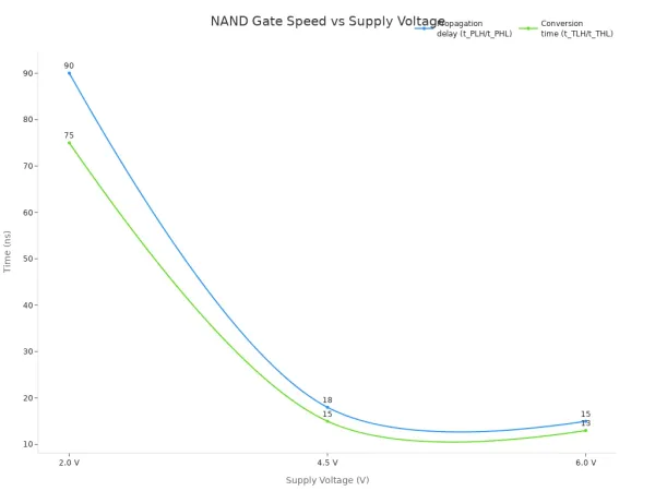
The table below shows how 4 input NAND gates perform in terms of power and speed:
| Parameter | Condition | Value |
|---|---|---|
| Static power consumption | CMOS 4 two-input NAND gate IC | ≤ 2 µA static current |
| Propagation delay (t_PLH/t_PHL) | Load capacitance = 50 pF | ≤ 90 ns at 2.0 V |
| ≤ 18 ns at 4.5 V | ||
| ≤ 15 ns at 6.0 V | ||
| Conversion time (t_TLH/t_THL) | Load capacitance = 50 pF | ≤ 75 ns at 2.0 V |
| ≤ 15 ns at 4.5 V | ||
| ≤ 13 ns at 6.0 V |
Constraints and Challenges
Despite their many benefits, 4 input NAND gates also present some challenges:
- Adding more inputs increases the number of transistors in series, which raises resistance and parasitic capacitance. This can slow down the gate’s response time.
- Propagation delay grows as the number of inputs increases. A 4 input NAND gate usually has a higher delay than a 2 input NAND gate.
- Larger device footprints can limit how many gates fit on a chip, especially in older or printed technologies.
- Complex gates may need higher voltage margins to avoid errors, which can stress the device and reduce its lifespan.
- Manufacturing costs for dual 4 input NAND gate ICs can range from $0.75 to $1.95 per unit, depending on the quantity purchased.
- In some organic or printed circuit technologies, 4 input NAND gates may switch more slowly and take up more space than silicon-based gates.
- Designers must carefully manage internal capacitances and input arrangements to keep power consumption and speed at optimal levels.
| Aspect | Explanation / Observation |
|---|---|
| Transistor Configuration | More NMOS transistors in series increase resistance and delay. |
| Parasitic Capacitance | More parallel transistors at the output increase capacitance and slow transitions. |
| Delay Relationship | Propagation delay increases with more inputs, often more than linearly. |
Note: While 4 input NAND gates are efficient and flexible, designers must balance speed, size, and power when using them in advanced digital systems.
The 4 input NAND gate stands as a versatile and essential component in digital electronics.
- Henry M. Sheffer proved its universality in 1913, allowing engineers to build any logic circuit using only NAND gates.
- Charles Sanders Peirce and George Boole laid the foundation for logic gates, which Claude Shannon later applied to electrical circuits.
- Modern chips like the 74LS38 and SN74LS00N use quad NAND gates to simplify design and improve reliability.
Students can explore resources such as Nand2Tetris and textbooks on CMOS logic to learn more about NAND gates and their applications in digital systems.
FAQ
What does a 4 input NAND gate do?
A 4 input NAND gate checks four signals. It gives a high output unless all four inputs are high. If every input is high, the output becomes low.
Can a 4 input NAND gate replace other logic gates?
Yes. Engineers can use only NAND gates to build any other logic gate. This makes the NAND gate a universal gate in digital electronics.
Where do engineers use 4 input NAND gates?
Engineers use these gates in alarm systems, memory circuits, and control panels. They help check many conditions at once and save space on circuit boards.
How do you make a 4 input NAND gate with 2 input NAND gates?
Connect two 2-input NAND gates to handle pairs of inputs. Feed their outputs into a third NAND gate. This setup works like a single 4 input NAND gate.
What is the Boolean expression for a 4 input NAND gate?
| Inputs | Boolean Expression |
|---|---|
| A, B, C, D | Y = NOT (A AND B AND C AND D) |
This formula shows how the gate works with four inputs.