What Determines SPI Speed A Complete Guide
The Serial Peripheral Interface (SPI) is famous for high-speed data transfer. This synchronous communication protocol enable
The Serial Peripheral Interface (SPI) is famous for high-speed data transfer. This synchronous communication protocol enables efficient data transfer between devices, with some data transfer rates exceeding 100 MHz. So, why doesn't your project's performance always hit these top data transfer rates? Your true SPI speed and overall throughput are limited by three key areas.
💡 The final performance of any SPI data transfer is a balance of your devices' hardware limits, the physical connection quality, and your software configuration.
Key Takeaways
- Your SPI speed depends on three main things: your devices' hardware limits, the quality of your physical connections, and how you set up your software.
- Always check the speed limits in the datasheets for both your master and slave devices. The slowest device sets the maximum speed for your SPI bus.
- Good PCB design is important. Keep wires short, match trace lengths, and use a strong ground plane to prevent signal problems at high speeds.
- Use Direct Memory Access (DMA) in your software for the best performance. DMA lets your microcontroller send data quickly without slowing down the main processor.
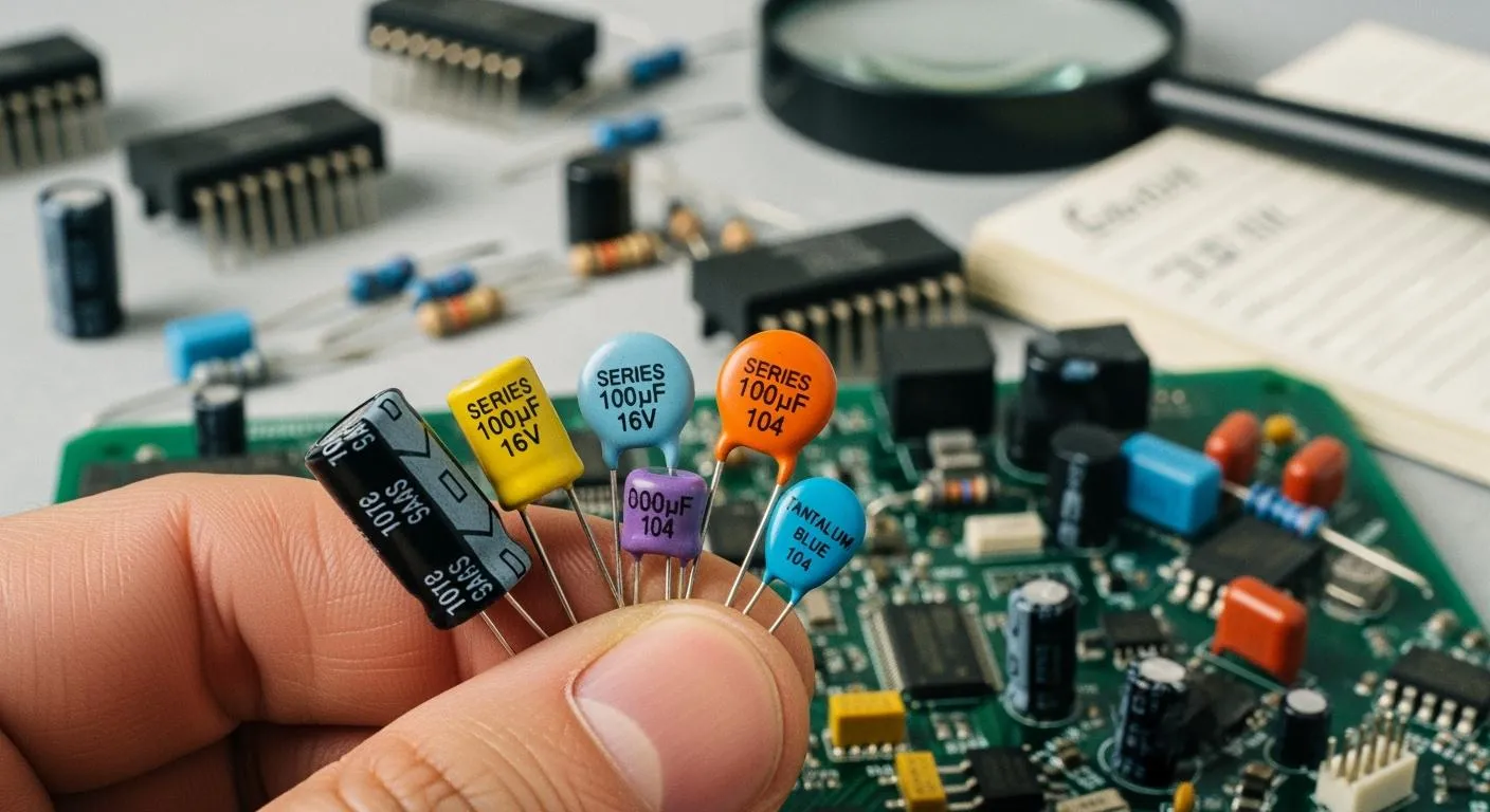
Hardware's Role in SPI Speed
The first step to understanding your system's maximum SPI speed is to look at the hardware itself. Before you even write a line of code or design a PCB, the datasheets for your master and slave devices set a hard upper limit. Your final performance is fundamentally tied to the capabilities of these integrated circuits.
Master Clock Limits
Your master device, typically a microcontroller, generates the SPI clock (SCK). This device has a maximum frequency at which it can operate its serial peripheral interface. You can find this limit in the electrical characteristics section of its datasheet. The tables often specify the maximum fSCK (SPI clock frequency) under different operating voltages.
For example, a microcontroller's datasheet might present its SPI characteristics like this:
| Symbol | Parameter | Conditions | Min | Typ | Max | Unit |
|---|---|---|---|---|---|---|
| fSCK | SPI clock frequency | Controller receiver mode 2.7 V <VDD< 3.6 V | - | - | 45 | MHz |
| Controller transmitter mode 2.7 V <VDD< 3.6 V | - | - | 45 | MHz |
Note: The values in the table above are based on
fPCLKx/3, wherefPCLKxis the peripheral clock. The actual maximum value depends on the microcontroller's specific architecture.
The master's own system clock also plays a role. The SPI peripheral often runs on a clock derived from the main system clock.
- A microcontroller's internal clock architecture may limit the SPI module's input clock. For instance, a module might only accept a maximum input of 48 MHz.
- This input clock is then divided down to generate the final SCK signal for the SPI transfer.
- This means even if the SPI peripheral can theoretically run faster, its performance is capped by the clock you feed it.
Slave Clock Constraints
Now, consider the slave device. Every SPI slave, whether it's a sensor, memory chip, or another microcontroller, also has a maximum clock frequency it can handle. This is often the most significant bottleneck in a master/slave configuration. Exceeding this limit will cause the slave to misinterpret data, leading to data corruption during the transfer.
💡 Your SPI bus is only as fast as its slowest device. The final communication speed must be set to the lower of the two maximums (master or slave).
You must carefully check the slave's datasheet. You might find different maximum data transfer rates depending on the operation. For example, an STM32 microcontroller in slave mode might support 40 MHz for receiving data but a lower speed like 24 MHz for full-duplex communication. These differences can arise from the internal logic required to sample and send data simultaneously. For most SPI slave devices, a safe rule of thumb is to keep the SPI clock rate below one-tenth of the slave's own system clock frequency to ensure a reliable data transfer.
Slave Processing Delays
A high clock frequency does not always equal high throughput. The true measure of performance is how much data you can transfer over time. Many slave devices need a pause between transactions to process information. This is known as slave processing time or inter-transaction delay.
Imagine you send a command to a sensor. The sensor needs time to perform a measurement before it has data ready for the next transfer. A fast SPI clock is useless if the master has to wait a long time for the slave to be ready. This delay dramatically impacts your overall data throughput.
Some common scenarios requiring this delay include:
| Scenario | Why a Delay is Needed |
|---|---|
| Slave has slow internal logic | The device needs time to process the previous byte of data. |
| Multi-frame SPI protocols | The protocol itself requires a specific time gap between frames. |
| SPI Flash page writes | The memory chip must pause to latch an address before writing data. |
| Avoiding timing errors | A small delay can help prevent errors at very high SPI clock speeds. |
So, how do you know when the slave is ready for the next transfer? Devices use several methods to signal their status:
- Busy Pin: Some devices have a dedicated output pin that they assert to signal they are busy processing.
- Status Register: You can poll a status register on the slave. This register often contains bits like
trdy(transmit ready) orrrdy(receive ready) to indicate its state. - Interrupts: The slave can use these status bits to trigger an interrupt on the master, actively signaling that it is ready for the next SPI transaction.
The Serial Peripheral Interface Physical Layer
Once you understand the limits of your integrated circuits, you must look at the physical connections between them. The printed circuit board (PCB) traces and wires that form your SPI bus are not perfect conductors. At high frequencies, these physical paths introduce their own set of challenges that can degrade signal quality and limit your overall performance.
Signal Path and Layout
Long wires and PCB traces can act like tiny antennas. This behavior introduces propagation delay, which is the time it takes for a signal to travel from the master to the slave devices. At low speeds, this delay is negligible. At high data transfer rates, it becomes a major problem.
Mismatches in trace length between the clock (SCK) and data (MOSI/MISO) lines cause timing errors. The clock signal might arrive at the receiver at a different time than the data. This can cause the slave device to latch the wrong data bit, corrupting the entire transfer. As your signal frequency increases, the clock period gets shorter, making your design much more sensitive to even small differences in propagation delay.
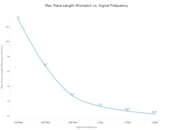
The table below shows how quickly the tolerance for trace length mismatch shrinks as the SPI clock frequency rises.
| Signal Frequency | Clock Period (T) | Max Skew Tolerance (20% T) | Propagation Delay (FR4) | Max Trace Length Mismatch |
|---|---|---|---|---|
| 100 MHz | 10 ns | 2 ns | ~150 ps/in | ~13 in |
| 200 MHz | 5 ns | 1 ns | ~150 ps/in | ~6.7 in |
| 500 MHz | 2 ns | 0.4 ns | ~150 ps/in | ~2.7 in |
| 1 GHz | 1 ns | 0.2 ns | ~150 ps/in | ~1.3 in |
| 2 GHz | 0.5 ns | 0.1 ns | ~150 ps/in | ~0.67 in |
| 5 GHz | 0.2 ns | 0.04 ns | ~150 ps/in | ~0.27 in |
Pro Tip: When your SPI bus operates in the 50-100 MHz range, you should treat the traces as transmission lines. To prevent signal reflections and ringing, you can add small series termination resistors (e.g., 22-33Ω) near the driver pins. Place them on the SCK, MOSI, and CS lines at the master and on the MISO line at each slave.
Bus Capacitance and Integrity
Every element on your PCB, from the IC pins to the traces themselves, adds a small amount of unwanted capacitance. This is called parasitic capacitance. It exists between the signal trace and its nearest reference plane, usually the ground plane. While you cannot eliminate it, you must manage it.
This capacitance directly impacts your signal's rise time. The rise time is how quickly the signal can transition from a low voltage to a high voltage. High bus capacitance acts like a hurdle, resisting the signal's ability to rise. This slows down the rise time and rounds the sharp edges of your clock signal. If the clock edge becomes too slow, the slave device may fail to register it correctly, limiting your maximum clock rate. Interestingly, capacitance has a much smaller effect on the signal's fall time.
Adding more slave devices to the SPI bus increases the total load capacitance, which can further degrade signal integrity. You can control this parasitic effect through careful PCB design.
- Use thinner surface layer laminates to reduce the distance to the adjacent ground plane.
- Choose low-Dk (dielectric constant) materials for your PCB to lower the total capacitance.
- Select components with smaller lead sizes to minimize their contribution.
Crosstalk and Noise
Crosstalk happens when the electromagnetic energy from one signal trace "leaks" into a neighboring trace. On a PCB, this often occurs between two SPI traces running side-by-side. This coupled energy creates noise on the "victim" trace. If the noise is large enough, it can cause false signal transitions and corrupt your data transfer.
This phenomenon is primarily due to capacitive coupling. The best way to fight crosstalk and other external noise is with a well-designed ground plane.
A solid ground plane provides a low-impedance return path for signal currents. This tightens the electromagnetic fields around the signal trace, containing them and preventing them from interfering with other signals. A closer reference plane leads to tighter coupling and less noise.
To improve your design and achieve higher data transfer rates, you should:
- Maximize your ground plane: Use as much free space on the PCB as possible for the ground plane.
- Use dedicated ground layers: In multi-layer boards, a dedicated ground plane provides excellent separation and reduces noise.
- Add stitching vias: If you must split a ground plane, use vias to "stitch" the separate areas together, creating a continuous, low-impedance path.
By carefully managing your PCB layout, capacitance, and grounding, you can preserve signal integrity. This allows you to run your SPI bus at a higher spi speed and achieve better overall throughput.
Software's Impact on SPI Performance
Your hardware and PCB layout set the potential for high-speed communication, but your software determines if you can actually achieve it. The choices you make in your code, from basic protocol settings to data handling methods, directly control your final SPI performance and throughput.
SPI Mode and Timing
The SPI protocol is synchronous, meaning the master and slave devices must agree on timing. You configure this timing by selecting the correct SPI mode. A mismatch here will cause the transfer to fail entirely. The mode is defined by two parameters in the slave device's datasheet:
- Clock polarity (CPOL): This sets the clock signal's idle state (low or high).
- Clock phase (CPHA): This determines if data is sampled on the first (leading) or second (trailing) clock edge.
These two settings combine to create four possible SPI modes. If your master is set to Mode 0 (CPOL=0, CPHA=0), it expects to sample data on a rising clock edge. Your slave device must also be configured for this mode to ensure a successful data transfer. Getting this wrong is a common source of errors that prevents communication between devices.
Driver and OS Overhead
How your microcontroller moves data has a huge impact on performance. You generally have two choices for handling an SPI transfer: interrupts or Direct Memory Access (DMA). Using interrupts is simpler for a basic transfer, but it creates significant CPU overhead that limits your maximum data transfer rates. For high performance, DMA is the superior method.
💡 DMA allows the SPI peripheral to transfer data directly to or from memory without involving the CPU. This frees the CPU to perform other tasks, dramatically increasing your system's efficiency and enabling a higher data rate.
The table below compares the two approaches:
| Feature | Interrupt-Driven SPI | DMA-Driven SPI |
|---|---|---|
| CPU Overhead | High; CPU manages every byte transfer. | Low; CPU is free after starting the transfer. |
| Throughput | Lower; Limited by CPU's ability to service interrupts. | Higher; Can reach the maximum SPI speed. |
| Use Cases | Good for low-rate sensors or simple commands. | Ideal for high-speed streaming and large data blocks. |
When you need to achieve the highest data transfer rates from components like high-resolution ADCs or flash memory, you should use DMA. This approach minimizes software delays and allows your SPI bus to operate closer to its hardware limits.
Your final SPI speed depends on three key factors. These are your hardware's limits, your physical connections, and your software's efficiency. You must consider all three areas to achieve the high data transfer rates SPI is known for. A fast system requires a complete approach.
💡 Actionable Takeaway: To find your true maximum speed, first check the slave device's datasheet for its speed limit. Next, test this speed with your PCB layout and software. Adjust downwards from there to find the fastest stable rate for your specific project.