Exploring the Advanced Features of the AD9081 Mixed Signal Front End
The AD9081 delivers a breakthrough for high-performance RF systems by combining high-speed ADC and DAC cores, advanced DSP,

The AD9081 delivers a breakthrough for high-performance RF systems by combining high-speed ADC and DAC cores, advanced DSP, and wide bandwidth on a single chip. Designers benefit from simplified architectures, lower power, and enhanced flexibility in demanding applications. Market trends show strong adoption of mixed-signal front ends in RF, driven by rapid 5G and automotive growth. Key features such as 12 GSPS DACs, 4 GSPS ADCs, and on-chip DSP reduce external components and power needs.
Key Takeaways
- The AD9081 integrates high-speed ADCs, DACs, and advanced DSP on a single chip, simplifying RF system design and reducing board size and power consumption.
- Its wide bandwidth and fast sampling rates support demanding applications like 5G, radar, and broadband communications with improved signal quality and flexibility.
- Built-in DSP features reduce the need for external processing, enabling efficient, scalable, and low-power system architectures.
- Multi-channel synchronization and advanced clocking ensure precise timing and phase alignment, critical for phased arrays and MIMO systems.
- The AD9081’s high integration and performance increase call capacity in wireless networks and enable compact, reliable, and future-ready RF solutions.
AD9081 Mixed-Signal Front End Highlights
High-Speed ADC and DAC Cores
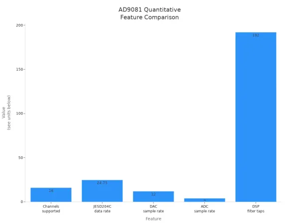
The AD9081 model stands out in the field of high-performance mixed-signal front ends by integrating both high-speed analog-to-digital and digital-to-analog conversion on a single chip. This integration supports demanding RF applications that require rapid sampling and precise signal fidelity. The device features four 12-bit, 4 GSPS RF analog-to-digital converters and four 16-bit, 12 GSPS RF digital-to-analog converters, enabling engineers to address complex signal environments with confidence.
- The AD9081 evaluation board offers flexible modes and configurations, including on-board clocking and FPGA interfacing.
- Software tools such as ACE and DPGDownloaderLite allow users to capture ADC data and generate DAC vectors, making performance analysis straightforward.
- The evaluation platform enables benchmarking of the ADC and DAC cores in real-world scenarios, such as aerospace radar, mmWave communications, and advanced instrumentation.
ADIsimPLL modeling of the AD9081’s sampling clocks demonstrates that simulated results closely match bench measurements. This precision confirms the reliability of the device’s sampling clock, which is essential for high-speed data conversion. Analog Devices’ RF ADCs, like the AD9213, achieve RF sampling up to 7 GHz, setting industry benchmarks that the AD9081 matches. The AD9175, a related DAC, supports sample rates up to 12.6 GSPS, highlighting the advanced speed capabilities present in the AD9081’s digital-to-analog cores.
The AD9081’s high-speed sampling enables engineers to design systems for radar, communications, and test equipment that demand both speed and accuracy.
Advanced DSP Integration
The AD9081 integrates advanced digital signal processing directly into its mixed-signal front end. This architecture includes four 16-bit, 12 GSPS RF digital-to-analog converters and four 12-bit, 4 GSPS RF analog-to-digital converters. These high-speed, high-resolution cores allow the device to handle complex signal generation and acquisition tasks, supporting ultrawideband RF applications.
- Embedded DSP features include programmable filtering, digital downconversion, and gain control within the ADC path.
- The DSP integration shifts processing from external FPGA fabric to the device itself, improving system power efficiency.
- In a 16-channel S-band direct sampling receiver, combining multiple channels improves noise density by nearly 10log(N), enhancing noise performance.
- Spurious signals decrease when channels are combined, resulting in better dynamic range.
- Amplitude and phase stability remain consistent, with amplitude stability within thousandths of a dB and phase stability within tenths of a degree, thanks to the device’s PLLs.
- Intermodulation products remain correlated across channels, showing the limits of linearity improvements from channel combination.
This level of DSP integration allows the AD9081 to deliver enhanced dynamic range, improved noise performance, and scalable system design for phased array and broadband applications.
Wide Bandwidth Performance
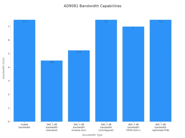
The AD9081 achieves exceptional bandwidth, making it a leader among mixed-signal front ends. The device supports wide instantaneous bandwidth, which is critical for modern RF systems that require high data throughput and flexible frequency coverage.
| Parameter | AD9081 Specification |
|---|---|
| ADC cores | Four 12-bit ADCs, 4 GSPS each |
| DAC cores | Four 16-bit DACs, 12 GSPS each |
| Usable bandwidth (DAC & ADC) | Up to 7.5 GHz with proper balun and PCB design |
| DAC 3 dB bandwidth | Up to 4.5 GHz (standard), 5.25 GHz (with inverse sinc correction), 7.5 GHz (2nd Nyquist zone) |
| ADC 3 dB bandwidth | Near 7 GHz with TCM1-83X+ balun, >7.5 GHz with optimized PCB and balun |
| Maximum external clock frequency | Up to 12 GHz |
This wide bandwidth supports a range of application scenarios:
| Application Scenario | Benefit from Wide Bandwidth Performance |
|---|---|
| Wireless communications infrastructure | Supports wide instantaneous bandwidth processing for high data rates |
| Microwave point-to-point, E-band, 5G mmWave | Enables broadband signal processing in high-frequency communication |
| Broadband communications systems | Handles wideband signals for improved throughput and capacity |
| DOCSIS 3.1 and 4.0 CMTS | Supports broadband cable modem termination systems with wide bandwidth |
| Phased array radar and electronic warfare | Low latency and frequency hopping modes for advanced radar and EW |
| Electronic test and measurement systems | Wideband ADC/DAC for accurate signal capture and generation |
The AD9081’s wide bandwidth, combined with its high-performance sampling and advanced DSP, enables engineers to build systems for 5G, radar, and broadband communications that demand both speed and flexibility. The device’s capabilities set a new standard for mixed-signal front ends, making it a preferred choice for next-generation RF designs.
Mixed-Signal Technology Overview
Mixed-Signal Front Ends in RF Applications
Mixed-signal front ends serve as the bridge between the analog world and digital processing in modern RF systems. These devices combine analog-to-digital converters and, in some cases, digital-to-analog converters on a single chip. They capture real-world signals, such as radio waves, and convert them into digital data for further processing. This integration remains essential because every RF system must first handle analog signals before digital processing can occur.
Mixed-signal front ends play a critical role in enabling high data transfer speeds, wide bandwidth, and high spectral efficiency. For example, platforms like Analog Devices' Apollo MxFE support advanced applications in phased array radar, electronic surveillance, and emerging 6G communications. Modern RF systems, such as MIMO communication devices and phased-array radar, often require multiple synchronized front ends. Tools like Tektronix's Spectrum View allow engineers to analyze multiple channels in real time, making it easier to manage complex RF signal chains and ensure system performance.
Note: Mixed-signal front ends drive innovation in 5G, IoT, automotive radar, and satellite communications by providing the necessary link between analog signals and digital processing.
System Integration Benefits
The evolution of mixed-signal front ends has transformed RF system design. Early RF systems had limited tuning ranges and fixed frequencies, which restricted flexibility. The introduction of software-defined radios allowed engineers to reconfigure systems through software, expanding tuning ranges and improving frequency agility.
- Modern mixed-signal devices now support operation from DC to microwave frequencies.
- Integration of digital signal processing and FPGAs enables complex modulation and adaptive processing.
- Multi-channel architectures with high sampling rates allow simultaneous processing of multiple signals.
Advances in processing power and miniaturization have made these devices smaller and more efficient. Software tools, including open-source platforms, have accelerated innovation and made advanced RF technology more accessible. These developments have improved flexibility, efficiency, and performance in applications such as military communications, telecommunications, radar, and 5G networks.
AD9081 Architecture and Features
Real-Time DSP Functions
The AD9081 stands out with its powerful on-chip digital signal processing. Engineers can use real-time DSP functions to manage signal conditioning, filtering, and frequency translation directly within the device. The architecture supports four main datapaths for wideband signals and eight channelizers for narrowband signals. Each datapath stage includes an independently tunable numerically controlled oscillator. This design allows users to process individual RF bands separately and align data rates with specific bandwidth requirements. The flexible interpolation and decimation factors help optimize performance for different applications.
Tip: Real-time DSP functions reduce the need for external processing hardware, saving board space and power.
Power Amplifier Protection and Monitoring
System designers often worry about protecting power amplifiers in high-performance RF systems. The AD9081 provides built-in monitoring features that help safeguard these critical components. The device can track signal levels and detect faults in real time. Engineers can set thresholds for automatic shutdown or alert generation if the system detects abnormal conditions. This protection helps prevent damage and extends the life of expensive RF amplifiers.
- Continuous monitoring ensures reliable operation.
- Automatic fault detection reduces downtime.
- Integrated protection features simplify system design.
Programmable GPIO and Control
The AD9081 offers programmable GPIO and control interfaces for flexible system integration. Designers can configure these interfaces to manage external devices, trigger events, or synchronize operations. The device supports multiple control modes, making it easy to adapt to different application needs.
| Feature | Benefit |
|---|---|
| Programmable GPIO | Customizable system control |
| Multiple control modes | Easy integration with other ICs |
| Synchronization | Reliable timing across channels |
The quad-channel tx rx architecture enables simultaneous transmission and reception, which is essential for modern RF systems. The on-chip clock multiplier generates sampling clocks up to 12 GHz, supporting both DAC and ADC cores. These features make the AD9081 a versatile solution for advanced RF applications.
Clocking and Synchronization

Low Phase Noise and PLL
The AD9081 uses advanced clocking technology to support high performance sampling clock requirements in demanding RF systems. Engineers rely on precise clock signals to achieve accurate data conversion and maintain signal integrity. The device features an analog phase detector PLL paired with a high-quality voltage-controlled oscillator. This combination delivers low phase noise, which is essential for high-speed sampling and clean signal output.
The following table summarizes key PLL and phase noise characteristics:
| Aspect | Details |
|---|---|
| PLL Type | Analog phase detector PLL with high-quality VCO (e.g., HMC1166) or DRO locked with analog PLL |
| Phase Noise Improvement | Analog PD PLL offers 10 to 20 dB in-loop phase noise improvement over conventional active PFD-based PLL synthesizers |
| Measured Phase Noise Results | Using HMC1166 VCO with analog PLL shows ~15 dB improvement compared to HMC440-based implementation at 1 GHz PD frequency |
| Clock Dominance Offset Range | Clock dominates phase noise from 200 kHz to 2 MHz offset with worst-case DAC additive noise degradation ~10 dB |
| DRO PLL Performance | DRO locked analog PLL nearly makes clock phase noise invisible under DAC additive phase noise, achieving very low jitter and phase noise suitable for high-performance synthesizers |
| System-Level Impact | Enables system-level clocking with very low jitter and phase noise, critical for microwave synthesizers, fast frequency hopping, and agile RF applications |
| Mixer Synthesizer Approach | Coarse/fine mixer synthesizer avoids phase noise and spur degradation from frequency multiplication, preserving DAC's additive phase noise performance at system output |
| Frequency Hopping | Supports ~300 ns agile frequency hopping with maintained phase coherency among multiple NCOs |
This performance allows the AD9081 to deliver a high performance sampling clock with very low jitter. System designers can achieve fast frequency hopping and maintain spectral purity. The device supports applications that require both wide bandwidth and precise timing.
Note: Low phase noise and stable PLL operation help engineers reduce errors during sampling and improve overall system accuracy.
Multichip Sync Capabilities
Modern RF systems often use multiple data converters in parallel. Synchronization between these devices is critical for phased array antennas, MIMO systems, and broadband receivers. The AD9081 provides robust multichip sync features to align sampling clocks and data paths across several devices.
- Engineers can synchronize multiple AD9081 chips using JESD204C interfaces.
- The device supports deterministic latency, which ensures that all channels sample signals at the same instant.
- Built-in synchronization logic helps maintain phase alignment, even during fast frequency changes.
These capabilities allow system architects to scale up channel counts without losing timing accuracy. The high performance sampling clock architecture ensures that every device in the system operates in harmony. This level of synchronization is vital for applications like radar, 5G base stations, and electronic warfare, where precise timing and phase coherence drive system performance.
10GHz Bandwidth and Application Scope
Wide Instantaneous Bandwidth
The AD9081 stands out by supporting a maximum instantaneous bandwidth of up to 2.4 GHz per data converter. This wide instantaneous bandwidth allows engineers to capture and process large portions of the spectrum without the need for multiple devices. The 10ghz bandwidth capability enables direct RF conversion for systems with an input range of dc to 18ghz. This approach reduces the size, weight, and power requirements of advanced systems.
Wide instantaneous bandwidth helps engineers design flexible systems that can adapt to new standards and future needs.
The device’s scalable on-chip digital signal processing works with high-speed sampling to handle wide signal bandwidths. This combination opens new possibilities in aerospace, defense, and instrumentation. For example, phased array radar and collision avoidance radar benefit from the ability to process broad frequency bands in real time. In security, mmwave imaging systems use this bandwidth to deliver clear, detailed images. Instrumentation fields, such as X-ray spectroscopy and food inspection, also rely on this performance for accurate results.
Use Cases in 5G and Broadband
The AD9081 plays a key role in modern communications infrastructure. Wireless equipment manufacturers use it in both 4G LTE and 5G mmwave radios. The 10ghz bandwidth allows multiband radios to fit into the same space as single-band radios. This design increases call capacity in 4G LTE base stations by up to three times.
A 1.2 GHz channel bandwidth supports the high data rates and radiodensity needed for new 5G networks. The device’s fast sampling and wide instantaneous bandwidth make it ideal for broadband applications that demand high throughput. Engineers can deploy the AD9081 in systems where enhanced capacity and flexible frequency coverage are critical.
| Application Area | Benefit from AD9081 |
|---|---|
| 5G Base Stations | Higher call capacity, multiband support |
| Broadband Communications | Increased data rates, flexible deployment |
| mmWave Radios | Compact design, wide frequency coverage |
Comparing Mixed-Signal Front-End Devices
Performance Benchmarks
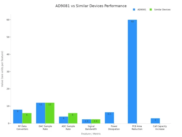
Engineers often compare mixed-signal front-end devices by looking at key performance metrics. The AD9081 stands out in the field of rf systems because it combines high channel count, wide bandwidth, and advanced digital features. The device integrates eight rf data converters—four transmit and four receive channels—within a single package. Competing devices, such as the AD9082, offer fewer channels in the same footprint. Both devices deliver 16-bit DACs at 12 GSPS, but the AD9081 provides more channels for multichannel operation.
The AD9081 supports an instantaneous signal bandwidth of up to 2.4 GHz. This wide bandwidth simplifies hardware design and supports advanced wireless applications. The device also features a JESD204C/B data interface, which enables high data rates for demanding systems. On-chip digital signal processing allows engineers to configure filters and perform digital up/down conversion, reducing the need for external processing.
| Feature / Metric | AD9081 | Similar Devices (e.g., AD9082) | Performance Advantage / Benchmark Summary |
|---|---|---|---|
| Number of RF Data Converters | 8 (4 Tx + 4 Rx) | 6 (4 Tx + 2 Rx) | Higher integration enables multichannel operation in same footprint |
| DAC Resolution and Sample Rate | 16-bit DACs at 12 GSPS | 16-bit DACs at 12 GSPS | Equal DAC specs, but AD9081 has more channels |
| ADC Resolution and Sample Rate | 12-bit ADCs at 4 GSPS | 12-bit ADCs at 6 GSPS | Slightly lower ADC sample rate but more ADC channels |
| Instantaneous Signal Bandwidth | Up to 2.4 GHz | Up to 2.4 GHz | Industry’s widest bandwidth simplifies hardware design |
| Power Dissipation | 6-7 W | N/A | 10X power reduction compared to FPGA-based architectures |
| PCB Area Reduction | 60% reduction compared to alternatives | N/A | Smaller footprint and integration reduce board complexity |
| Call Capacity Increase for 4G LTE | Up to 3X increase | N/A | Enables multiple radios in single footprint |
| Data Interface | JESD204C/B (up to 24.75 Gbps/lane) | JESD204C/B | Supports high data rates for advanced applications |
| On-chip DSP and Configurability | Yes, supports configurable filters and digital up/down conversion | N/A | Enhances flexibility and reduces external processing needs |
Integration and Power
The AD9081 leads in integration among mixed-signal front-end devices. Its design reduces printed circuit board area by up to 60% compared to alternatives. This high level of integration allows engineers to build compact rf systems with less complexity. The device also delivers a significant power advantage. Power dissipation ranges from 6 to 7 watts, which represents a tenfold reduction compared to traditional FPGA-based architectures.
High integration and low power help engineers create efficient, scalable systems for next-generation wireless and radar applications.
The AD9081 enables higher call capacity in 4G LTE base stations, supporting up to three times more calls in the same footprint. Its flexible on-chip digital signal processing further reduces the need for external components. These features make the AD9081 a top choice for designers who need high performance, efficiency, and flexibility in modern rf systems.
System Design Benefits
Reduced Component Count
The AD9081 helps engineers simplify their designs by reducing the number of components needed in RF systems. By integrating high-speed ADCs, DACs, and advanced DSP blocks on a single chip, the device eliminates the need for multiple discrete converters and external signal processing hardware. This integration leads to smaller printed circuit boards and fewer interconnections, which lowers the risk of signal loss and interference.
- Engineers can replace several chips with one AD9081, streamlining the signal chain.
- Fewer components mean less board space and lower assembly costs.
- The simplified design improves reliability and shortens the time needed for troubleshooting.
A compact system design also reduces power consumption. Lower power requirements help engineers meet strict energy budgets in applications like 5G base stations, radar, and portable test equipment. The AD9081’s high level of integration supports dense, high-performance systems without the complexity of traditional multi-chip solutions.
Enhanced Flexibility
The AD9081 gives system engineers greater flexibility when building advanced RF systems. The device’s hardened DSP blocks inside the digitizer IC reduce the need for external FPGA resources. This feature simplifies the signal chain and allows engineers to focus on system-level innovation.
- The Quad MxFE Platform, which uses four AD9081 chips, supports scalable multichannel systems. Engineers can implement amplitude and phase equalization for phased array, radar, satellite communication, and electronic warfare.
- The platform reduces system-level power consumption and shortens development time.
- Engineers can use the complete system solution and software platform to develop proprietary algorithms and speed up time to market.
- The design supports easier calibration and beamforming algorithm development, including multi-chip synchronization.
- Measurements show about 10 dB improvement in noise density and better spurious performance when combining channels, which boosts dynamic range.
The AD9081 enables engineers to validate new beamforming technologies and develop software before custom hardware becomes available. This flexibility supports rapid prototyping and faster deployment in complex RF environments.
The combination of integrated DSP, high-speed data interfaces, and scalable architecture makes the AD9081 a top choice for engineers who need efficient, adaptable, and future-ready system designs.
The AD9081 delivers practical advantages for RF and data converter system designers. Its high integration, wide bandwidth, and advanced DSP enable multi-band radios to fit into compact spaces, support small antenna deployments, and shift complex filtering into the digital domain.
- Multi-band radios increase call capacity by three times in 4G LTE base stations.
- Compact integration reduces size, weight, and power for wireless infrastructure.
- Direct sampling architectures simplify design and reduce noise.
Future mixed-signal front ends will support higher frequencies and more flexible, software-defined radios, driving innovation in telecommunications and high-performance electronics.
FAQ
What makes the AD9081 different from other mixed-signal front ends?
The AD9081 combines high-speed ADCs and DACs with advanced DSP on one chip. This integration reduces board size and power use. Engineers can design more compact and flexible RF systems.
Can the AD9081 support multi-channel applications?
Yes. The AD9081 offers four transmit and four receive channels. Engineers can build systems for phased arrays, MIMO, or broadband communications. The device supports synchronized operation across all channels.
How does the AD9081 help lower system power consumption?
The AD9081 integrates converters and DSP blocks. This design removes the need for extra chips and external processing. As a result, total system power drops by up to 10 times compared to traditional solutions.
Is the AD9081 suitable for 5G and broadband systems?
Absolutely. The AD9081 supports wide bandwidth and fast data rates. Engineers use it in 5G base stations, broadband radios, and advanced test equipment. The device handles demanding wireless and data converter tasks with ease.