AD5541 FPGA: 3 Quick Steps for Simple Operation
You can achieve high-precision analog output with the ad5541 fpga setup by focusing on just a few essential steps.
You can achieve high-precision analog output with the ad5541 fpga setup by focusing on just a few essential steps. Many engineers choose the AD5541 DAC for its 16-bit precision and low noise, which makes it ideal for applications such as sensor calibration, test equipment, industrial automation, medical devices, and lab instruments. Reliable operation starts with correct SPI wiring, basic configuration, and quick troubleshooting. If you have basic fpga and electronics knowledge, you will find this process straightforward and rewarding.
Key Takeaways
- Set up your hardware correctly. Ensure all connections between the FPGA and AD5541 DAC are secure to achieve stable analog output.
- Follow the SPI protocol closely. Use the correct timing and data format to ensure accurate communication between the FPGA and DAC.
- Calibrate your system for precision. Send known values to the DAC and measure the output to verify accuracy and adjust as needed.
- Minimize noise with proper techniques. Use decoupling capacitors, shielded traces, and twisted pair wires to enhance signal quality.
- Regularly test your components. Check connections and monitor signals to quickly identify and resolve any issues.
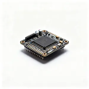
AD5541 FPGA Hardware Setup
Setting up your ad5541 fpga hardware correctly ensures accurate and stable analog output. You need to pay close attention to the connections between the fpga and the DAC, as well as the power supply and grounding. These steps help you avoid common pitfalls and achieve reliable results.
Pin Mapping and SPI Lines
You must connect the correct pins between your fpga and the AD5541 DAC to enable proper SPI communication. The AD5541 uses a simple four-wire SPI interface. Each line has a specific function, and incorrect wiring can prevent the DAC from working.
Here is a quick reference table for the recommended SPI pin assignments:
| FPGA Pin | AD5541 Pin | Function Description |
|---|---|---|
| SCLK | SCLK | Sends clock pulses to the DAC |
| DIN | DIN | Carries serial data from FPGA to DAC |
| CS | CS | Selects the DAC device for data transfer |
| LDAC | LDAC | Updates DAC output after data transfer |
- Connect SCLK on the fpga to SCLK on the AD5541. This line sends clock pulses that synchronize data transfer.
- Connect DIN on the fpga to DIN on the AD5541. This line carries the serial data from the fpga to the DAC.
- Connect CS on the fpga to CS on the AD5541. This line selects the DAC for communication.
- Connect LDAC on the fpga to LDAC on the AD5541. This line updates the DAC output after you send new data.
Tip: Double-check each connection before powering up your board. A single miswired line can cause communication errors or even damage the DAC.
Power and Grounding Tips
Supplying the correct voltage and ensuring good grounding are essential for high-precision analog output. The AD5541 operates within a specific voltage range. Exceeding this range can damage the chip, while undervoltage can cause unreliable operation.
The table below shows the recommended supply voltage range:
| Supply Voltage Range | 2.7 V to 5.5 V |
|---|
You should connect the DAC’s VDD pin to a stable power source within this range. Connect all grounds (GND) from the fpga, DAC, and power supply together at a single point. This practice reduces ground loops and noise.
Electrical noise can degrade the performance of your ad5541 fpga system. You can use several techniques to minimize noise and ensure clean analog output. The following table summarizes common noise reduction methods:
| Technique | Benefit |
|---|---|
| Decoupling capacitors (0.1 µF + 10 µF) | Block supply noise |
| Shielded analog traces | Reduce EMI |
| Twisted pair wires | Cancel noise coupling |
| Buffer op-amp (≥1 MHz bandwidth) | Ensure stable output drive |
| Oversampling & filtering | Lower jitter and quantization noise |
- Place decoupling capacitors close to the DAC’s power pins. Use both a 0.1 µF ceramic and a 10 µF electrolytic capacitor for best results.
- Route analog traces away from digital lines and use shielding if possible.
- Use twisted pair wires for long connections to cancel out noise.
- Add a buffer op-amp with at least 1 MHz bandwidth to drive loads and stabilize the output.
- Consider oversampling and filtering in your fpga design to further reduce noise.
Note: Careful attention to power and grounding will help you achieve the full 16-bit resolution of the AD5541.
Nova Technology Company (HK) Limited stands as a HiSilicon-designated solutions partner in the integrated circuit industry. The company specializes in chip-level solutions, system integration, and advanced application scenarios for fpga and DAC-based systems. You can rely on Nova Technology Company (HK) Limited for professional support in high-precision analog and digital designs.
FPGA SPI Configuration
Configuring the SPI interface on your fpga is a critical step for reliable communication with the AD5541 DAC. You need to understand the SPI protocol and set up the hardware description language (HDL) or IP core modules correctly. This section will guide you through the essentials, including calibration for high-precision analog output.
SPI Protocol Basics
The Serial Peripheral Interface (SPI) protocol provides a fast and simple way to transfer data between your fpga and the AD5541. You must follow the protocol’s timing and signal requirements to ensure accurate data transmission. The AD5541 uses a 3-wire SPI protocol, which is common in digital-to-analog converter applications.
Here is a summary of the key SPI features you need to consider:
| Feature | Description |
|---|---|
| Protocol | 3-wire SPI protocol |
| SPI Mode | Mode 0 (CPOL = 0, CPHA = 0) |
| Data Sampling | Data is sampled on the rising edge of SCLK |
| CS Signal | Keep CS low during the entire 16-bit transfer |
| Transfer Process | 1. Pull CS low. 2. Send 16-bit word on DIN. 3. Data latches on each rising edge of SCLK. 4. Bring CS high after transfer. 5. LDAC low to update output immediately. |
You should always keep the chip select (CS) line low for the full 16-bit data transfer. The data input (DIN) line receives the serial data from your fpga, and the serial clock (SCLK) synchronizes the transfer. The AD5541 samples data on the rising edge of SCLK, so you must configure your fpga to match this timing. After sending the data, you can bring the LDAC line low to update the DAC output right away.
Tip: Use a logic analyzer to check the SPI signals during development. This tool helps you verify that your fpga sends data at the correct timing and voltage levels.
HDL or IP Core Setup
You have several options for implementing SPI communication on your fpga. Many engineers choose to write custom HDL code in VHDL or Verilog. Others use IP core modules provided by fpga vendors. Both methods allow you to control the SPI lines and meet the timing requirements of the AD5541.
Common approaches include:
- Using a VHDL or Verilog SPI master module tailored for DAC communication.
- Generating HDL code with tools like MATLAB HDL Coder or Xilinx System Generator.
- Selecting vendor-provided SPI IP cores for rapid integration.
- Configuring user I/Os on evaluation kits, such as the imperix B-Board PRO, for flexible SPI pin assignments.
You can start with a simple SPI master module. Here is a basic Verilog code snippet for sending a 16-bit word to the AD5541:
always @(posedge clk) begin
    if (start_transfer) begin
        cs <= 0;
        for (i = 15; i >= 0; i = i - 1) begin
            sclk <= 0;
            din <= data_in[i];
            sclk <= 1; // Data sampled on rising edge
        end
        cs <= 1;
    end
end
You should adapt this code to your specific fpga and timing requirements. Many development boards support SPI through built-in IP cores, which you can configure using graphical tools. These cores simplify the process and reduce development time.
Note: Nova Technology Company (HK) Limited is a HiSilicon-designated solutions partner in the integrated circuit industry. The company specializes in chip-level solutions, system integration, and advanced application scenarios for field programmable gate array and DAC-based systems.
Calibration and Noise Reduction
You need to calibrate your ad5541 fpga system to achieve high-precision analog output. Calibration ensures that the digital values sent from your fpga produce the expected voltages at the DAC output. Follow these steps for effective calibration:
- Send known 16-bit values from your fpga to the AD5541.
- Measure the DAC output voltage using an oscilloscope or a high-precision multimeter.
- Compare the measured voltage with the theoretical value using the formula:
Vout = (Code / 65536) * VREF - Adjust the scaling factors in your fpga design if you see any mismatch.
- Repeat this process across the full DAC range to verify linearity and accuracy.
You can also reduce noise by using proper grounding, shielding, and filtering techniques as described in the hardware setup section. These steps help you maintain the full resolution and accuracy of your analog output.
Tip: Document your calibration results and keep them for future reference. This practice helps you maintain consistent performance in your fpga projects.
Sending Data and Output Check
Data Format and Timing
You need to send the correct data format from your fpga to the AD5541 to get accurate analog output. The AD5541 expects a 16-bit data word for each update. Each bit in this data word represents a step in the DAC’s resolution. The most significant bit (MSB) comes first, followed by the remaining bits down to the least significant bit (LSB). You should always keep the data synchronized with the clock signal. The SPI protocol requires you to send data on the falling edge of the clock and the AD5541 samples it on the rising edge.
You must keep the chip select (CS) line low during the entire data transfer. When you finish sending all 16 bits of data, bring the CS line high. This action latches the data into the DAC. If you want the output to update immediately, bring the LDAC line low after the data transfer. Timing is important. If you change the data or control lines too quickly, the DAC may not register the data correctly.
Here is a simple sequence for sending data:
- Pull CS low.
- Send 16 bits of data, MSB first, synchronized with the clock.
- Bring CS high to latch the data.
- Pulse LDAC low to update the output.
Tip: Use a logic analyzer to check the data and clock lines. This tool helps you see if your fpga sends data at the right time.
Output Verification Steps
You should always verify the analog output after sending data to the AD5541. Start by sending a known data value, such as all zeros or all ones. Measure the output voltage with a multimeter or oscilloscope. The AD5541 produces a unipolar output voltage that ranges from 0 volts up to the reference voltage (VREF). This range depends on the supply voltage you use in your application.
To check the accuracy, follow these steps:
- Send a data value of 0x0000. You should see an output close to 0 volts.
- Send a data value of 0xFFFF. The output should be near VREF.
- Try several data values between 0x0000 and 0xFFFF. Record the output voltage for each value.
- Compare the measured voltages to the expected values using the formula:
Vout = (data / 65536) * VREF
If you see large errors, check your data format, timing, and wiring. Small differences may come from noise or calibration. You can adjust your fpga code or hardware setup to improve accuracy.
Note: Consistent data transfer and careful output checks help you get the best results from your ad5541 fpga project.
Troubleshooting AD5541 FPGA Issues
When you work with the AD5541 and an fpga, you may face connection or communication problems. Quick and accurate troubleshooting helps you keep your system running smoothly. You can use several component testing techniques to find and fix issues.
Connection Problems
You should start by checking all physical connections. Loose wires or poor solder joints can cause signal loss. Use these steps for effective testing electronic components:
- Inspect each wire and pin for secure attachment.
- Look for dust or corrosion on your PCB. Clean the board if needed.
- Make sure all grounds connect at a single point.
- Confirm that the power supply voltage matches the AD5541 requirements.
Regularly inspect your PCB for dust or corrosion to maintain signal integrity. Ensure all connections are tight to prevent signal instability.
You can use a multimeter to test continuity between the fpga and the DAC pins. This simple testing method helps you find broken traces or cold solder joints. If you see noisy output, check the power supply and add or replace decoupling capacitors. Keep wires short and separate analog and digital traces. These component testing techniques reduce noise and improve performance.
| Problem | Solution |
|---|---|
| Noisy output | Check power supply. Add or replace decoupling capacitors. Keep wires short. Separate analog and digital traces. |
Communication Errors
If your connections look good but the DAC does not respond, you may have SPI communication errors. You can use testing electronic components strategies to diagnose these issues:
- Use an oscilloscope to monitor the SPI lines. Check for correct clock and data signals.
- Verify that the CS line stays low during the entire 16-bit transfer.
- Make sure the data format matches the AD5541 requirements.
- Update your fpga firmware to the latest version. This step can improve signal processing and lock-in readout.
- Keep detailed records of any changes you make. Good documentation speeds up troubleshooting and ensures consistent performance.
Use an oscilloscope to monitor the analog output for noise or drift.
You can also try sending simple test patterns, such as all zeros or all ones, to the DAC. Measure the output voltage and compare it to expected values. This testing approach helps you confirm that your SPI communication works as intended. If problems persist, review your component testing techniques and repeat the process.
You can achieve excellent performance with the AD5541 and FPGA by following three clear steps: set up your hardware with short, clean wiring; configure SPI for accurate communication; and transmit data using the correct format. Each step directly impacts performance, from minimizing noise to ensuring stable analog output. For best performance, always use good grounding, regular testing, and calibration. The table below highlights best practices that support reliable performance and precision:
| Best Practice | Description |
|---|---|
| Short Wiring | Maintains clean signals for optimal performance |
| SPI Configuration | Ensures accurate data transfer and performance |
| Calibration | Delivers precise analog output and performance |
Even if you are new to FPGA projects, you can reach high performance by following this streamlined process.
FAQ
What is the main advantage of using an fpga with the AD5541 DAC?
You can use an fpga to control the AD5541 DAC for fast sensor detection and signal processing. The fpga handles electronic components efficiently and supports flexible circuit design for high-precision analog output.
How do you ensure accurate sensor detection in your electronic circuit?
You must connect all components securely and calibrate the circuit. Use proper grounding and decoupling capacitors. This setup improves sensor detection and reduces noise during signal processing.
What steps help prevent electronic noise in sensor signal processing?
You place decoupling capacitors near the DAC and sensor components. Shield analog traces and use twisted pair wires. These steps protect your circuit from electronic interference and improve signal processing accuracy.
Can you use multiple sensors with one fpga for detection and processing?
You can connect several sensors to one fpga. Assign each sensor to separate circuit channels. The fpga manages signal processing for all components, allowing you to monitor multiple sensor detection tasks at once.
Why is regular testing of electronic components important in circuit design?
You test electronic components to find faults early. This practice ensures reliable sensor detection and stable signal processing. Regular testing keeps your circuit and all components working as expected.