

Forget complex schematics a simple CY7C68001 circuit diagram.
This simple cy7c68001 circuit diagram shows everything you need. It establishes
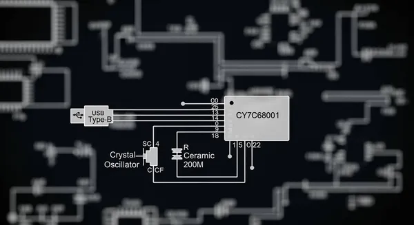

This simple cy7c68001 circuit diagram shows everything you need. It establishes basic high-speed USB communication for modern hobbyist projects. Many older designs include extra components that are not essential for getting started.
Goal: The main objective is to build a functional board quickly. This minimal design helps you bypass unnecessary complexity and focus on core functionality. You can get your project up and running in no time.
Key Takeaways
- The CY7C68001 chip connects parallel devices to high-speed USB 2.0.
- A stable 3.3V power supply with capacitors is important for the chip to work well.
- The D+ and D- lines need careful design for good USB data transfer.
- A 24MHz crystal provides the exact timing the chip needs to operate.
- An I2C EEPROM stores the device's identity for the computer to recognize it.
Your minimal CY7C68001 circuit diagram
Let's break down the schematic into its core functional blocks. Understanding the role of each part is key to building a successful device. This minimal cy7c68001 circuit diagram is designed for simplicity and rapid prototyping.
The CY7C68001 high-speed USB controller
The CY7C68001 is the heart and brain of our circuit. This powerful chip acts as a bridge. It connects a parallel interface (like from an FPGA or another microcontroller) to a high-speed USB 2.0 port. Its main job is to handle all the complex USB protocol requirements for you.
The EZ-USB SX2™ (the family this chip belongs to) is specifically engineered for this purpose. It integrates a USB transceiver and a Serial Interface Engine (SIE) to manage data flow. This allows your main processor to simply send data to the CY7C68001's memory buffer, or FIFO. The chip then takes care of transmitting it over USB at up to 480 Mbps.
Here are some key specifications for the CY7C68001-56PVC model:
| Feature | Specification |
|---|---|
| USB Speed | High-Speed (480 Mbps) or Full-Speed (12 Mbps) |
| Operating Voltage | 3.0V to 3.6V |
| I/O Tolerance | 5V Tolerant Inputs |
| FIFO Space | 4 KB shared across four configurable endpoints |
| Package | 56-pin SSOP (or QFN) |
Note: The 5V tolerant I/Os are a fantastic feature. They allow you to directly connect the chip to older 5V logic devices without needing level-shifter ICs, which simplifies your design.
Stable 3.3V power supply and decoupling
A stable power source is non-negotiable for any high-speed digital circuit. The CY7C68001 operates on a 3.3V supply. While it can tolerate a range from 3.0V to 3.6V, a regulated 3.3V source is ideal for stable performance.
You will notice several capacitors connected to the power pins in the schematic. These are called decoupling capacitors.
- 10µF Capacitor: This larger capacitor acts as a small local power reservoir. It smooths out larger, slower fluctuations in the power supply.
- 0.1µF Capacitors: These smaller capacitors are placed as close as possible to each power pin on the IC. They filter out high-frequency noise generated by the chip's own rapid switching.
Think of them as a shock absorption system for your power lines. They ensure the chip receives clean, steady electricity, which is essential for preventing data errors at 480 Mbps. The power section of the cy7c68001 circuit diagram is simple but absolutely vital for reliable operation.
USB D+ and D- data lines
The D+ (Data Plus) and D- (Data Minus) lines are the physical pathway for all USB data. They must be treated with care. These two traces form a "differential pair," which means they work together to transmit data robustly and cancel out electromagnetic interference.
For USB 2.0 High-Speed mode, several rules are critical:
- Impedance Matching: The traces on your PCB must have a specific differential impedance of 90 ohms (Ω) with a tolerance of about ±15%. This prevents signal reflections that can corrupt your data. Achieving this involves carefully controlling trace width and the spacing between the D+ and D- traces.
- Series Resistors: The schematic shows small resistors (typically 22Ω to 27Ω) placed in series on the D+ and D- lines, close to the CY7C68001 pins. These resistors help match the output impedance of the chip to the transmission line impedance, which is crucial for maintaining signal integrity.
- PCB Layout: The physical routing of these traces is just as important as the components.
- Keep the D+ and D- traces as short and direct as possible.
- Route them parallel to each other with a constant spacing.
- Avoid sharp 90-degree bends; use two 45-degree bends or a gentle curve instead.
- Route them over a solid ground plane to provide a clear return path for the signal.
Correctly implementing these data lines is arguably the most important part of a functional high-speed cy7c68001 circuit diagram.
Essential peripherals for functionality
The CY7C68001 chip is powerful, but it cannot work alone. It relies on a few external components to function correctly. These peripherals provide the essential clock signal, identity, and stability needed for any USB device. Think of them as the mandatory support systems for our chip's brain.
The 24MHz crystal oscillator
The CY7C68001 needs a precise and stable clock signal to operate. This is the "heartbeat" of the chip. A 24MHz crystal oscillator provides this timing reference. The chip uses an internal Phase-Locked Loop (PLL) to multiply this 24MHz signal up to the 480MHz required for high-speed USB operations.
The accuracy of this crystal is not just a recommendation; it is a strict requirement. The tolerances of the clock source directly impact the stability of USB devices.
- High-speed USB requires a minimum frequency accuracy of 0.25%.
- The crystal and its two loading capacitors (C1 and C2 in the schematic) form a resonant circuit.
- These capacitors must be chosen carefully to match the crystal's specified load capacitance. An incorrect value can "pull" the frequency off its target, causing communication to fail.
For High-Speed USB, the frequency tolerance is even tighter than for Full-Speed.
| USB Type | Frequency Tolerance |
|---|---|
| Full-Speed (FS-USB) | ±0.25% or 2,500 ppm |
| High-Speed (HS-USB) | ±500 ppm |
This tight tolerance of ±500 ppm for High-Speed USB means you must ensure the crystal is correctly loaded. A small change in load capacitance can significantly affect the frequency. For example, a 10% change in capacitance can cause a frequency shift of about 20 ppm. This is a large portion of the total tolerance budget. Always check your crystal's datasheet for the correct load capacitor values.
I2C EEPROM for USB identity (VID/PID)
When you plug a USB device into your computer, the operating system asks, "Who are you?" The device answers with two numbers: a Vendor ID (VID) and a Product ID (PID). This VID:PID pair is stored in a small I2C EEPROM chip connected to the CY7C68001.
The CY7C68001 is designed to automatically look for an EEPROM on its I2C bus (SCL and SDA pins) at startup. If it finds one with a valid signature, it loads the VID, PID, and other configuration data from it. If it finds no EEPROM, it enumerates with a default Cypress VID/PID.
Why is this important? A unique VID:PID pair allows the operating system to identify your specific device and load the correct driver for it.
Here are some key facts about the VID and PID:
- They are used to differentiate your USB device from all others.
- They do not define the device's function or communication protocol.
- The device's function (e.g., a logic analyzer or a camera) is defined by its class descriptors, which are also often stored in the EEPROM.
- In Windows, you may need a simple
.inffile to tell the OS that your device with its specific VID:PID should use a particular driver.
For hobbyist projects, you can use a VID:PID pair designated for testing. For commercial products, you must purchase a VID from the USB Implementers Forum (USB-IF).
The basic reset circuit
A reset circuit ensures the microcontroller starts in a known, stable state. When power is first applied, the voltage does not instantly jump to 3.3V. It ramps up. During this ramp-up, the chip can behave unpredictably. A reset circuit holds the chip in a reset state until the power supply is stable.
Our minimal cy7c68001 circuit diagram shows a simple approach, but a more robust solution is highly recommended.
| Feature | Simple RC Reset Circuit | Dedicated Supervisor IC (e.g., MAX809) |
|---|---|---|
| Reliability | Less reliable, sensitive to noise and slow power ramps. | Very reliable, with precise voltage monitoring. |
| Functionality | Provides a basic power-on reset pulse. | Monitors Vcc and generates a perfect reset signal. |
| Best Use | Simple, non-critical projects. | Any application where reliability is important. |
While a simple Resistor-Capacitor (RC) circuit is cheap, it is often unreliable. It is much more difficult to achieve consistent behavior with RC resets, which can lead to unpredictable startup problems. For this reason, beginners should avoid them.
Pro Tip: Use a dedicated supervisor IC like a MAX809 or TPS3823. These 3-pin components are inexpensive and simple to add. They monitor the supply voltage and hold the
RESET#pin low until the voltage is stable, guaranteeing a clean startup every time. This small addition dramatically improves the reliability of your device.
Practical application: A DIY logic analyzer
Theory is great, but practical application is where the fun begins. One of the most popular projects for the CY7C68001 is a DIY logic analyzer. This powerful tool lets you "see" digital signals, making it invaluable for debugging communication protocols like I2C, SPI, or UART. Our minimal circuit provides the perfect hardware foundation for this project.
Connecting the parallel interface
The CY7C68001's parallel interface pins (the GPIOs) become the input channels for your logic analyzer. You can directly connect these pins to the digital signals you want to monitor on your target device. The chip's General Programmable Interface (GPIF) is what makes this high-speed data capture possible.
The GPIF is a highly configurable engine inside the chip. It acts as a smart state machine that can be programmed to automatically read data from the parallel pins and store it in the FIFO buffer.
- The GPIF enables a direct, "glueless" connection to many parallel interfaces.
- It uses programmable waveform descriptors to define how and when to capture data.
- This allows the chip to interface with standards like ATA and UTOPIA without needing extra logic chips.
For a simple logic analyzer, you just connect the CY7C68001's data pins (e.g., FD0-FD7) to your target's signal lines.
Interfacing with Sigrok and PulseView
Your CY7C68001 board is the hardware, but you need software on your PC to control it and visualize the data. This is where the open-source project Sigrok comes in. PulseView is a part of Sigrok that provides a user-friendly graphical interface.
When you connect your board to the PC, a special firmware is first loaded onto the CY7C68001. This firmware configures the GPIF and makes the device behave like a standard logic analyzer.
The key is the fx2lafw firmware and driver. PulseView uses this generic driver to communicate with any compatible FX2-based device, including our CY7C68001 board. It allows the software to see your DIY hardware as an 8-channel, 24MHz logic analyzer, ready to capture signals.
Once connected, you can set your sample rate, trigger conditions, and start capturing data. PulseView will then display the digital signals as clean waveforms, helping you debug your projects with ease. 📈
The simple cy7c68001 circuit diagram you have seen is a powerful foundation. It provides everything needed for modern high-speed USB projects. You can now build custom peripherals, perhaps for high-speed data transmission at rates like 60 Mbyte/s, or interface with PC software.
Your journey into custom USB hardware starts now. Grab your components, fire up your soldering iron, and start experimenting with your own board! 🛠️
FAQ
Can I use a different crystal frequency?
No, you must use a 24MHz crystal. The CY7C68001's internal PLL is specifically designed to multiply a 24MHz input to the 480MHz required for high-speed USB. Using another frequency will prevent the USB interface from working correctly.
Is the I2C EEPROM really necessary?
The chip will function without an EEPROM. It will enumerate with a default Cypress Vendor ID and Product ID. However, for your PC to recognize it as a specific device (like a logic analyzer), you need the EEPROM to store a unique VID:PID pair.
Why is a supervisor IC better than an RC reset?
A supervisor IC provides a much more reliable reset. It precisely monitors the voltage and only releases the reset pin when the power is stable. An RC circuit is sensitive to power supply ramp-up times and noise, which can cause startup failures.
Pro Tip: For a reliable device, always use a dedicated supervisor IC. A
MAX809or similar component is a small investment for guaranteed stability. ⚙️
Can I power this circuit directly from USB?
Yes, you can. The USB port provides a 5V supply. You will need a Low-Dropout (LDO) voltage regulator to step the 5V down to the stable 3.3V required by the CY7C68001 chip. A common choice for this is the AMS1117-3.3.
