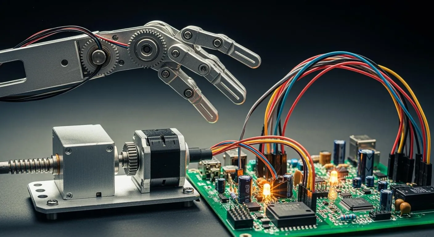
4 Transistors That Power Versatility in Contemporary Electronics
The 4 transistors—Bipolar Junction Transistor (BJT), Field-Effect Transistor (FET), Metal-Oxide-Semiconductor FET (MOSFET),
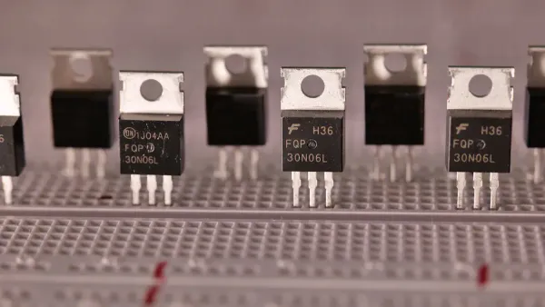
The 4 transistors—Bipolar Junction Transistor (BJT), Field-Effect Transistor (FET), Metal-Oxide-Semiconductor FET (MOSFET), and Insulated-Gate Bipolar Transistor (IGBT)—stand as the fundamental building blocks behind the rise of integrated circuits and the miniaturization of electronics. These types of transistors have shaped the invention of the transistor era and remain small but versatile components in electronic devices. As fundamental components of modern electronics, they enable energy-efficient designs and drive innovation. Together, these 4 transistors serve as the basic building blocks of digital electronics, supporting the ongoing evolution of modern electronics.
Key Takeaways
- The four main transistors—BJT, FET, MOSFET, and IGBT—are essential building blocks in modern electronics, enabling devices to amplify and switch electrical signals efficiently.
- BJTs control current with a small base current and are great for analog circuits and audio amplifiers, while FETs use voltage control, offering high input impedance and low power use, ideal for digital and low-noise applications.
- MOSFETs feature a four-terminal design that allows fast switching and energy-efficient operation, making them perfect for microprocessors, memory chips, and compact electronic devices.
- IGBTs combine features of BJTs and MOSFETs to handle high voltage and current, powering electric vehicles, industrial machines, and renewable energy systems with reliable performance.
- Choosing the right transistor depends on the application needs like switching speed, power handling, and cost; together, these transistors drive innovation and support the growth of technologies like IoT, AI, and sustainable electronics.
Bipolar Junction Transistor (BJT)
Structure
A Bipolar Junction Transistor (BJT) features three layers of semiconductor material. These layers form either an NPN or PNP arrangement. The structure includes:
- The emitter, which is heavily doped to inject charge carriers—electrons in NPN types and holes in PNP types—into the base.
- The base, which is thin and lightly doped. This design allows most carriers to pass through with minimal recombination, making the transistor efficient for microelectronics.
- The collector, which is larger and moderately doped. It collects carriers and can handle higher voltages and currents.
The arrangement and doping levels of these semiconductor regions influence the electrical characteristics of the transistor. The direction of current flow and the type of charge carriers differ between NPN and PNP types, affecting how the device operates in circuits. Manufacturing techniques such as ion implantation and thermal diffusion define the physical dimensions and doping profiles, which directly impact performance in microelectronics.
How Transistors Work: BJT
The BJT operates by controlling a large collector current with a much smaller base current. When the base-emitter junction receives a forward bias, the emitter injects charge carriers into the base. Because the base is very thin, most carriers move through it and reach the collector, which is reverse-biased. This process creates a collector current. A small change in base current can control a much larger collector current, allowing the transistor to amplify or switch electronic signals. In the active region, the device acts as an amplifier. In saturation or cutoff, it functions as a switch. This ability to control current flow makes BJTs essential in microelectronics.
Tip: Proper biasing ensures the transistor operates in the desired region, whether for amplification or switching.
Applications
BJTs play a vital role in many areas of microelectronics. Some key applications of transistors include:
- Audio amplifiers and signal-processing circuits, where high current gain and fast switching speeds are needed.
- Analog circuits such as operational amplifiers and voltage regulators, providing precise current control.
- Digital circuits, where BJTs act as switches to control binary states in computers and smartphones.
- Power supply units and inverters, converting AC to DC and vice versa.
- Radio-frequency circuits, including oscillators, mixers, and RF amplifiers.
BJTs remain relevant in modern electronics because they offer precise current control and high gain. Engineers use thermal management techniques like heat sinks to maintain performance. The evolution of transistor technology and its role in sustainable technologies further support the continued importance of BJTs in microelectronics.
Field-Effect Transistor (FET)
Structure
A Field-Effect Transistor (FET) uses three terminals: gate, source, and drain. The gate controls the flow of current between the source and drain by creating an electric field in the semiconductor channel. Unlike Bipolar Junction Transistors, which use both electrons and holes as charge carriers, FETs rely on a single type of carrier. This unipolar design means the gate does not require a steady current, only a voltage. The gate is often insulated from the channel by a thin oxide layer, which increases input impedance and reduces power consumption. The structure of a FET allows it to operate efficiently in microelectronics, where low noise and high input impedance are essential.
| Aspect | Bipolar Junction Transistor (BJT) | Junction Field-Effect Transistor (JFET) |
|---|---|---|
| Structure | Three semiconductor layers forming two p-n junctions (emitter, base, collector) | Single type of semiconductor channel controlled by gate voltage (gate, source, drain) |
| Charge Carriers | Both electrons and holes (bipolar) | Majority carriers only (unipolar) |
| Control Mechanism | Current-controlled (base current) | Voltage-controlled (gate-source voltage) |
| Input Impedance | Low | High |
| Noise Level | Higher noise | Lower noise |
| Power Consumption | Higher | Lower |
| Temperature Sensitivity | More sensitive | Less sensitive |
| Typical Applications | Analog amplification, power circuits | High-input impedance circuits, low-noise applications |
How Transistors Work: FET
FETs operate by using a voltage at the gate terminal to control the current between the source and drain. The gate voltage creates an electric field in the semiconductor channel, which changes its conductivity. This process does not require a continuous input current, unlike BJTs. The high input impedance of FETs makes them ideal for sensitive circuits in microelectronics. The relationship between gate voltage and drain current follows a square-law pattern, allowing precise control. Engineers use FETs to amplify or switch electronic signals in digital and analog circuits. The insulated gate design prevents charge-storage problems, enabling fast switching speeds in central processing units and memory chips.
Note: FETs provide better high-frequency response and lower noise than BJTs, making them suitable for modern microelectronics.
Applications
Field-Effect Transistors play a vital role in many sectors. They are essential in microelectronics for digital logic circuits, memory devices, and central processing units. FETs also support analog signal processing in audio equipment and sensors. The global market for FETs, especially MOSFETs, reached about $8 billion in 2023 and is projected to grow to $15 billion by 2032. This growth comes from demand in consumer electronics, automotive systems, telecommunications, and industrial automation.

FETs manage power in smartphones, laptops, and electric vehicles. They enable energy-efficient designs in renewable energy systems and smart factories. Asia-Pacific leads the market due to strong semiconductor manufacturing and high demand for consumer electronics. North America and Europe also show significant growth. The ability of FETs to amplify or switch electronic signals makes them indispensable in modern devices and supports their application in microelectronics across many industries.
Metal-Oxide-Semiconductor FET (MOSFET)
Four-Terminal Design
A MOSFET features four terminals: Gate, Source, Drain, and Substrate (Body). The gate sits above the semiconductor channel, separated by a thin oxide layer. This design allows the gate to control the electric field inside the semiconductor, which regulates current flow between the source and drain. The source and drain act as entry and exit points for charge carriers, while the substrate forms the body of the transistor and influences its electrical properties. Each terminal plays a unique role in device operation, scalability, and efficiency. Engineers use this four-terminal structure to manage short channel effects, which can occur when the gate loses control over the channel as devices shrink. Careful control of terminal interactions helps maintain performance as transistors become smaller, supporting the development of powerful and compact electronic devices.
Note: Advanced modeling of terminal charges and capacitances in MOSFETs enables accurate simulation and optimization for scalable, efficient semiconductor devices.
How Transistors Work: MOSFET
The MOSFET operates by using the gate voltage to create an electric field in the semiconductor channel. When the gate-to-source voltage exceeds a certain threshold, the field attracts charge carriers and forms a conductive channel between the source and drain. This process, called inversion, allows current to flow. By adjusting the gate voltage, the transistor can switch the current on or off rapidly, making it ideal for switching applications. Small changes in gate voltage also modulate the channel's conductivity, allowing the MOSFET to amplify or switch electronic signals. The insulated gate provides high input impedance, enabling fast switching and precise control with minimal power loss. This structure supports high-speed operation in modern electronics.
Versatility in Modern Electronics
MOSFETs play a central role in the miniaturization and efficiency of powerful and compact electronic devices. Their ability to switch and amplify signals at high speeds makes them essential in digital circuits, microprocessors, and memory chips. MOSFETs excel in low-voltage, high-frequency, and low-current applications, where energy efficiency is critical. The table below compares the efficiency of MOSFETs with BJTs and IGBTs in power electronics:
| Device Type | Power Dissipation Mechanism | Efficiency Characteristics | Application Suitability |
|---|---|---|---|
| MOSFET | Power loss as I² × R_DS(on); low ON resistance in low voltage | Highly efficient in low-voltage, high-frequency, low-current applications; requires heat sinks due to thermal limits | Switching power supplies (~100 kHz), low current density scenarios |
| BJT | Power loss as V_CE(sat) × I_C; higher conduction losses | Less efficient due to higher conduction losses; current-driven input control | Less favored in modern power electronics for efficiency reasons |
| IGBT | Low ON-state voltage drop; switching losses dominate but lower than MOSFET at high voltage/current | Superior thermal efficiency; often no heat sink needed; better in high voltage, high current, lower frequency applications | AC drives (<20 kHz), high current density, high voltage power electronics |
MOSFETs help engineers design powerful and compact electronic devices for smartphones, laptops, and renewable energy systems. Their four-terminal design and efficient operation support the ongoing advancement of modern electronics.
Insulated-Gate Bipolar Transistor (IGBT)
Structure
The Insulated-Gate Bipolar Transistor features a unique hybrid structure that combines elements from both MOSFETs and bipolar junction transistors. Its cell structure resembles an n-channel vertical power MOSFET but replaces the n+ drain with a p+ collector layer. This forms a vertical PNP bipolar junction transistor, resulting in a four-layer NPNP configuration. The device includes a MOSFET input stage and a bipolar output stage, with a p+ injection layer that enhances conduction. This design allows the transistor to handle very high voltage ratings, often above 1 kV, and high current ratings, sometimes exceeding 500 A. The voltage-controlled gate input provides high input impedance, while the bipolar output ensures low conduction losses. These features make the IGBT ideal for high power applications, where efficient conduction and voltage handling are critical.
Note: The hybrid structure of the IGBT enables it to balance high voltage and current handling with low on-state resistance, making it a key component in power electronics.
How Transistors Work: IGBT
The IGBT operates by integrating the high input impedance and voltage control of MOSFETs with the strong current handling of bipolar junction transistors. When a voltage is applied to the gate terminal, it creates an electric field that allows current to flow between the collector and emitter. The p+ injection layer reduces on-state resistance, enabling the device to conduct large currents efficiently. The transistor achieves high switching speeds and low voltage drops, which are essential for power electronics and switching applications. This combination of features allows the IGBT to perform well in circuits that require both fast switching and the ability to handle large amounts of power.
Applications
IGBTs play a vital role in many key applications of transistors, especially in power electronics. They are widely used in electric vehicles, industrial automation, renewable energy systems, and railway propulsion. In electric vehicles, IGBTs manage power conversion and battery systems. Renewable energy systems, such as solar and wind inverters, rely on these transistors for efficient grid connection. Industrial sectors use IGBTs in motor drives, robotics, and HVAC systems. Railway traction systems and commercial building infrastructure also depend on IGBTs for reliable operation. The market for IGBTs continues to grow, driven by the rise of electric vehicles, renewable energy, and smart grids. Technological advancements, such as new packaging and the use of silicon carbide materials, further improve their performance in high power applications. The ability of IGBTs to support high blocking voltages and fast switching makes them essential in modern electronic devices and power electronics.
4 Transistors Compared
Strengths
Engineers rely on different types of transistors because each offers unique strengths. The table below highlights the main advantages and weaknesses of each device:
| Device Type | Strengths | Weaknesses |
|---|---|---|
| Bipolar Junction Transistor (BJT) | High linearity, consistent gain, good for analog and low-noise circuits, affordable, strong in amplifiers | Needs constant base current, low input impedance, slower switching, can overheat, gain changes with temperature |
| Field-Effect Transistor (FET) | High input impedance, voltage-controlled, fast switching, low power use, low noise | Sensitive to static, needs careful voltage control, can distort analog signals |
| Metal-Oxide-Semiconductor FET (MOSFET) | Very fast switching, low on-resistance, high input impedance, great for digital and high-frequency circuits | Sensitive to static, can be costly, needs careful gate control |
| Insulated-Gate Bipolar Transistor (IGBT) | Handles high voltage and current, combines BJT and MOSFET benefits, efficient for power electronics | Slower switching than MOSFET, more complex, needs extra circuits to turn off |
BJTs show strong performance in analog and low-noise applications. MOSFETs and FETs excel in high-speed and high-frequency switching, which supports the rapid development of microelectronics. IGBTs work best in high-power and industrial settings.
Ideal Use Cases
Selecting the right transistor depends on the needs of the circuit. The table below summarizes key criteria:
| Criteria | BJTs | FETs/MOSFETs | IGBTs |
|---|---|---|---|
| Drive Method | Current-driven | Voltage-driven | Voltage-driven |
| Power Consumption | High | Low | Medium |
| Switching Speed | Slow | Fast | Medium |
| Voltage Handling | Good | Moderate | Excellent |
| Current Handling | Moderate | Moderate | Excellent |
| Cost | Low | Moderate | High (but cost-effective for high power) |
- BJTs suit audio amplifiers, analog circuits, and simple switches in microelectronics.
- FETs and MOSFETs power digital logic, memory chips, and high-frequency circuits like RF amplifiers.
- IGBTs drive electric vehicles, industrial motors, and renewable energy systems where high voltage and current are needed.
Tip: For high-frequency switching in microelectronics, MOSFETs offer the best performance. For high power and voltage, IGBTs are the top choice.
Engineers consider switching speed, voltage and current needs, cost, and reliability when choosing among these types of transistors. Each device supports the ongoing development of microelectronics by meeting specific application demands.
Role of Transistors in Modern Electronics
Fundamental Components of Modern Electronics
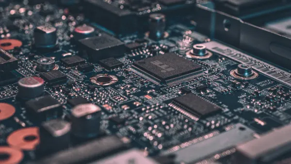
Transistors serve as the basic building blocks of digital electronics. They control the flow of electrical current, allowing devices to amplify or switch signals. This function supports the operation of integrated circuits, which can contain millions of transistors on a single chip. These integrated circuits enable the miniaturization and increased power of modern electronics, such as smartphones, computers, and medical equipment. Transistors also create switching circuits and logic gates, which form the core of digital computing. Their presence in microprocessors and memory chips highlights their role in the development of microelectronics. Academic and industry sources, including IEEE Spectrum and ScienceDirect, confirm that transistors are fundamental components of modern electronics. The invention of the transistor at Bell Labs and the MOSFET’s recognition by the US Patent and Trademark Office both underscore their impact on the electronics industry. These achievements show that transistors are an indispensable part of modern technology.
Note: Without transistors, the digital age would not exist. Every electronic device today relies on their ability to process and control signals.
Impact on Innovation
Advancements in transistor technology continue to drive innovation across many fields.
- Low-power transistors now support green computing and sustainable technologies.
- Flexible transistors on polymer materials make wearable electronics and personalized devices possible.
- Transistors enable the Internet of Things (IoT), powering sensor networks, wireless communication, and edge computing.
- These advances help create smart cities, improve agriculture, and support industrial automation.
Researchers have developed new types of transistors, such as negative-capacitance field-effect transistors, which lower power consumption and enable energy-efficient switching. The use of new materials like graphene and gallium nitride improves performance and reliability. These changes lead to faster processors, better medical devices, and more efficient renewable energy systems. The role of transistors in modern electronics ensures that innovation continues in computing, telecommunications, and sustainable energy. As technology evolves, transistors remain at the heart of progress, supporting the ongoing development of microelectronics and shaping the future of the electronics industry.
The 4 transistors drive versatility and innovation in modern electronics.
- Manufacturers use these devices to tailor solutions for consumer electronics, automotive, and telecommunications.
- Recent advances in materials like graphene and silicon carbide improve speed and efficiency, supporting compact and powerful devices.
- Ongoing research in transistor design and sustainability will shape the next generation of electronics, meeting demands for AI, IoT, and eco-friendly technology.
FAQ
What is the main difference between a BJT and a FET?
A BJT uses current to control current, while a FET uses voltage to control current. BJTs work well in analog circuits. FETs offer high input impedance and low power use, making them ideal for digital and low-noise applications.
Why do engineers prefer MOSFETs in digital circuits?
MOSFETs switch quickly and use little power. Their high input impedance allows for efficient signal control. Engineers choose MOSFETs for microprocessors, memory chips, and other digital devices that need fast and reliable switching.
Where do IGBTs provide the most benefit?
IGBTs excel in high-power and high-voltage applications. They power electric vehicles, industrial motors, and renewable energy systems. Their design allows for efficient energy conversion and reliable operation in demanding environments.
Can transistors be damaged by static electricity?
Yes, static electricity can damage transistors, especially MOSFETs and FETs. Engineers use grounding straps and antistatic mats to protect sensitive devices during handling and assembly.