NAND Flash Memory An In-Depth Analysis
The question of which nand flash memory is best depends entirely on an application's specific needs for cost, performance, a
The question of which nand flash memory is best depends entirely on an application's specific needs for cost, performance, and endurance. Designers use SPI NOR for reliable code execution. They use NAND for high-capacity data storage. The various nand flash memory types—SLC, MLC, TLC, and QLC—create a spectrum of these trade-offs. The NAND flash memory market's strong growth highlights the importance of choosing the right NAND solution for any project using NAND technology. The entire NAND flash memory ecosystem is expanding.
| Metric | Value |
|---|---|
| Market Size in 2025 | USD 85.84 Billion |
| Market Size in 2033 | USD 140.89 Billion |
| CAGR (2025-2033) | 6.39% |
This growth makes understanding NAND flash memory and each NAND variant critical.
Key Takeaways
- SPI NOR flash is good for running important code quickly. It helps devices start fast.
- NAND flash is best for storing lots of data. It is used in devices like SSDs.
- Different NAND types offer different benefits. SLC is strong and lasts long, while QLC stores a lot of data cheaply.
- The Flash Translation Layer (FTL) helps NAND memory work well. It makes sure the memory lasts longer.
- Choosing the right memory depends on what you need. Consider cost, speed, and how long the memory will last.
SPI NOR Flash: The Basics
SPI NOR flash memory serves a different purpose than NAND. Designers choose it for storing and executing critical code. Its architecture prioritizes reliability and fast random access over high-density storage. This makes it the foundation for fast-booting and stable embedded systems.
The Simple SPI NOR Command Set
SPI NOR flash uses a straightforward command set. A host processor can read data from any location by sending a simple read command and an address. This direct addressability is similar to RAM. It eliminates the need for complex management software like a Flash Translation Layer (FTL). This simplicity makes firmware development easier and more predictable.
Execute-in-Place (XIP) for Fast Boot
A key advantage of SPI NOR is its support for Execute-in-Place (XIP). XIP allows a processor to run program code directly from the flash chip. The system does not need to copy the code to RAM first. This capability enables nearly instant system startup. Many devices, from automotive dashboards to industrial controllers, rely on XIP for rapid boot performance.
Tip: Using XIP significantly reduces the amount of system RAM needed, which can lower the overall cost and complexity of a design.
SPI NOR Timing and Performance
Modern SPI NOR devices offer excellent read/write speeds. Interfaces like Quad-SPI (QSPI) and Octal-SPI (OSPI) use multiple I/O lines to increase data throughput. For example, some QSPI devices can support clock frequencies up to 200MHz in Double Data Rate (DDR) mode. Advanced Octal SPI flash can achieve continuous read data transfer rates of up to 240MB/s. These high read/write speeds ensure that code execution from flash does not create a system bottleneck.
High Endurance and Data Retention
Reliability is a core strength of SPI NOR flash. It offers high endurance, typically rated for at least 100,000 program/erase cycles per sector. This durability ensures the memory can handle frequent firmware updates over a product's lifespan. Furthermore, NOR flash provides excellent data retention, often guaranteed for over 20 years. This makes it a safe choice for storing essential bootloaders and configuration data that must never be lost.
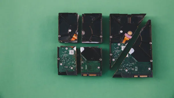
Deep Dive into NAND Flash Memory
Unlike NOR, the architecture of nand flash memory is optimized for high-density, low-cost storage. It excels at handling large, sequential blocks of data. This makes nand the standard for applications like a solid state drive (ssd). It does not, however, offer the fast, random-access capabilities of NOR flash. The entire non-volatile nand flash memory ecosystem is built around this design principle.
The NAND Command Set: Block and Page
Designers interact with nand flash memory through a block-and-page structure. Data is written and read in units called pages. Modern nand page sizes are often 4KB. These pages are grouped into larger units called blocks. A single block can contain up to 512 pages, reaching sizes of 8MB or more. A key rule of nand is that you can write to a page, but you can only erase an entire block. This write/erase asymmetry is a fundamental concept for any ssd.
The Role of the Flash Translation Layer (FTL)
The block-and-page complexity is hidden from the host system by a crucial piece of software: the Flash Translation Layer (FTL). The FTL makes the complex nand flash memory behave like a simple block device for the operating system. It manages all background operations to maintain performance and data integrity. Key FTL algorithms include:
- Wear-Leveling: This distributes write cycles evenly across all blocks. It prevents some blocks from wearing out faster than others.
- Garbage Collection: This process reclaims space from blocks containing invalid data. It moves valid data to a new block before erasing the old one. The FTL is the intelligence inside every modern solid state drive and ssd.
Introducing SPI NAND
SPI NAND combines the simple, low-pin-count Serial Peripheral Interface (SPI) with the high storage density of nand flash memory. This creates a cost-effective solution for embedded systems that need more storage than SPI NOR can offer but do not require the high performance of parallel nand. As a HiSilicon-designated solutions partner, Nova Technology Company (HK) Limited often helps designers integrate these advanced memory solutions into complex systems-on-a-chip (SoCs). This type of nand is ideal for data logging and storing media assets.
NAND Reliability Factors: Read Disturb
High-density nand flash memory faces reliability challenges that impact data integrity. One major issue is read disturb. Repeatedly reading a page can cause bit-flips in adjacent, unread pages within the same block. To counter this, nand controllers use powerful Error Correction Code (ECC) algorithms. The ECC requirement grows with nand density, which affects read/write speeds. This ensures long-term data integrity for the ssd.
ECC Requirements: SLC vs. QLC NAND
| Feature | SLC NAND | QLC NAND |
|---|---|---|
| ECC Requirement | Basic algorithms | Complex LDPC is a must |
| Error Rate | Lower | Higher |
| Complexity | Most basic design | Highest level of complexity |
This table shows how more complex nand requires stronger protection to guarantee data integrity in a solid state drive. The improved read/write speeds of modern nand are partly due to efficient ECC handling.
Endurance Compared: NOR vs. NAND
Designers must consider memory lifespan for system reliability. NOR flash generally offers higher endurance than nand flash memory. However, the story for nand is more complex. The specific type of nand flash memory determines its overall endurance and suitability for an application. This makes understanding the endurance spectrum crucial for ensuring long-term data integrity.
Defining Endurance: P/E Cycles
Flash memory cells wear out over time. The primary metric for measuring this lifespan is the program/erase (P/E) cycle. One P/E cycle involves writing data to a memory block and then erasing it. Each cycle causes a small amount of physical degradation to the cell's insulating oxide layer. A device's endurance rating indicates how many P/E cycles its cells can withstand before they become unreliable. This finite write endurance is a core characteristic of all nand technology.
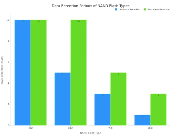
The NAND Endurance Spectrum
Different types of nand flash memory offer a wide range of endurance levels. Single-Level Cell (SLC) nand provides the highest endurance, while higher-density types trade endurance for lower cost. This trade-off directly impacts the expected lifespan and data integrity of a storage device.
| NAND Type | P/E Cycles |
|---|---|
| SLC | 100,000 |
| MLC | 3,000 |
Lower endurance also correlates with shorter data retention periods, another critical factor for data integrity. The ability of a nand cell to hold its charge degrades after many P/E cycles. This makes data integrity a major concern for lower-endurance nand flash memory.
Extending Lifespan with Wear-Leveling
Controllers use sophisticated techniques to maximize the limited endurance of nand. The most important technique is wear-leveling. This process ensures that write and erase operations are distributed evenly across all memory blocks. It prevents specific blocks from wearing out prematurely.
Advanced static and dynamic wear-leveling algorithms can nearly double the lifespan of a nand-based SSD. Some policies extend SSD endurance by up to 1.72 times compared to static wear-leveling alone.
Modern controllers also use advanced methods like the Write-Aware Re-shuffling Mechanism (WARM). These intelligent algorithms manage data placement to further improve endurance. This management is essential for maintaining data integrity over the product's entire lifecycle.
Which NAND Flash Memory is Best for Your Application?
Choosing the right nand flash memory requires a careful analysis of trade-offs. Each type offers a different balance of cost, performance, and endurance. Answering the question of which nand flash memory is best means matching your application's workload to the specific strengths of each technology. As a HiSilicon-designated solutions partner, Nova Technology Company (HK) Limited helps engineering teams navigate these choices to select the ideal memory for their designs.
An Overview of NAND Flash Memory Types
The nand flash memory market includes four main types: Single-Level Cell (SLC), Multi-Level Cell (MLC), Triple-Level Cell (TLC), and Quad-Level Cell (QLC). The primary difference is the number of bits stored in each memory cell. This directly impacts storage density, cost, and performance. Storing more bits per cell requires more precise voltage control, which increases the page programming time (tPROG) and lowers overall read/write speeds.
The cost per gigabyte decreases as the number of bits per cell increases. This makes QLC the most affordable option for high-capacity storage, while SLC remains the most expensive.
| Memory Type | Cost Per GB |
|---|---|
| SLC | Highest |
| MLC | High |
| TLC | Moderate |
| QLC | Lowest |
Currently, Triple-Level Cell (TLC) nand flash memory holds a dominant market share of over 38.09%. Its widespread adoption comes from its excellent balance of cost, capacity, and performance, making it suitable for a vast range of consumer and enterprise applications. Understanding which nand flash memory is best starts with this spectrum.
SLC: For Mission-Critical Embedded Systems
Single-Level Cell (SLC) nand stores one bit of data per cell. This simple design provides the fastest performance and the highest endurance. Industrial-grade SLC nand flash memory guarantees a write endurance between 50,000 and 100,000 program/erase (P/E) cycles. This durability makes it the top choice for applications where data integrity cannot be compromised. The high endurance ensures a long operational life even with frequent write operations.
SLC is the standard for systems that demand extreme reliability. Its superior data integrity and resilience make it essential for harsh environments.
- Defense & Aerospace: Used in unmanned aerial systems (UAS) for flight data logging.
- Robotics & Factory Automation: Found in industrial SD cards for robotic arms and PLCs.
- Medical Devices: Powers equipment where failure is not an option.
- Telecommunications Infrastructure: Ensures stability in network hardware.
MLC: A Balance of Performance and Cost
Multi-Level Cell (MLC) nand flash memory stores two bits per cell. It offers a middle ground between SLC and TLC. MLC provides good endurance and performance at a more accessible price point than SLC. This balance makes it a strong candidate for enterprise-grade solid state drive products and high-end consumer electronics. An MLC-based ssd delivers reliable performance for write-intensive workloads without the high cost of SLC. The technology provides a solid foundation for a durable solid state drive.
TLC: The Mainstream Consumer Standard
Triple-Level Cell (TLC) nand stores three bits per cell. This technology is the workhorse of the modern storage market. It powers the majority of consumer ssd devices and smartphones. TLC offers high storage densities at a very competitive cost. While its endurance is lower than SLC or MLC, it is more than sufficient for typical consumer use cases. A 1TB consumer-grade TLC ssd often has an endurance rating of 300 to 500 Terabytes Written (TBW). This level of endurance ensures years of reliable operation for gaming, content creation, and general computing. The excellent read/write speeds of a modern TLC ssd make it a popular choice. This type of nand flash memory is a key component in many ssd models.
QLC: For Read-Intensive, High-Capacity Archives
Quad-Level Cell (QLC) nand flash memory stores four bits per cell. This allows for massive storage capacities at the lowest cost per gigabyte. QLC is accelerating the replacement of hard disk drives (HDDs) in laptops, PCs, and gaming consoles. Its primary strength is storing large amounts of data that are written once and read many times. This makes a QLC ssd ideal for game libraries, media archives, and data backups. The technology is perfect for a high-capacity solid state drive.
However, QLC has the lowest endurance and slower sustained write performance. Answering which nand flash memory is best for write-heavy tasks would exclude QLC. Its lower endurance and impact on data integrity make it less suitable for such workloads.
Pro Tip: 💡 Once the internal cache of a QLC ssd is full, its write speeds can drop significantly. This happens when transferring very large files. For everyday tasks, this performance change is often not noticeable, but it is a critical factor for data-intensive applications. The read/write speeds are a major consideration.
The low cost of a QLC ssd makes high-capacity storage more accessible. This affordability drives the growth of the QLC market, especially for read-focused applications where data integrity and endurance are less critical than capacity. The read/write speeds are optimized for these use cases.
Designers make a clear choice for memory. They use SPI NOR for code execution and NAND for data storage. For example, a processor like the AM62Ax uses:
- SPI NOR Flash: For fast, reliable booting.
- NAND Flash Memory: For storing the bootloader and other data.
Selecting the right nand flash memory involves a direct trade-off between endurance, performance, and cost. The endurance of a nand flash memory device is a key factor. High endurance ensures data integrity. Low endurance reduces cost.
The final answer to which nand flash memory is best depends on the application. Designers must match their workload and budget to the specific strengths of each nand flash memory type to ensure optimal endurance and performance.
FAQ
Why do systems use both NOR and NAND flash?
Designers use both memory types for different jobs. SPI NOR flash enables fast system booting and reliable code execution. NAND flash provides high-capacity data storage for applications and user files. This division optimizes overall system performance and cost, with each memory serving a distinct purpose.
What is the main job of the Flash Translation Layer (FTL)?
The Flash Translation Layer (FTL) is essential software inside a storage device. It makes complex NAND memory appear as a simple block device to the operating system. The FTL manages background tasks like wear-leveling. This intelligent management ensures the long-term health of an ssd.
Which NAND type is best for a gaming PC?
TLC NAND is an excellent choice for a gaming PC. It offers a great balance of cost, performance, and capacity for modern gaming workloads. A TLC-based ssd loads games and applications quickly. QLC is also a good option for storing large game libraries that are read frequently.