The Future of Three-Dimensional Integrated Circuits in Smart Sensing Applications
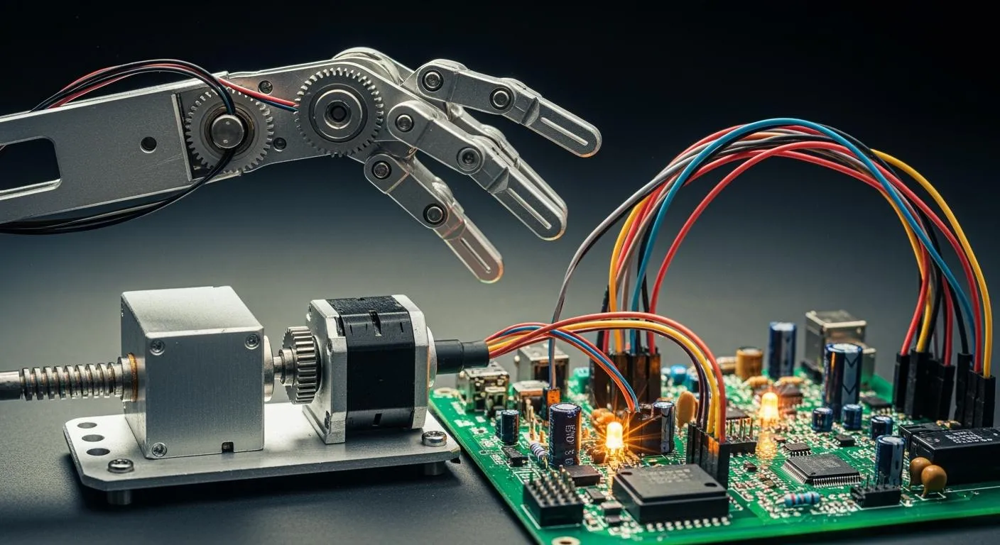
Three-dimensional integrated circuits are changing smart sensing. They help make devices small, strong, and work better. New progress shows microelectrodes made with CHIP processes work well.
Three-dimensional integrated circuits are changing smart sensing. They help make devices small, strong, and work better. New progress shows microelectrodes made with CHIP processes work well. They also fit into living tissues easily. Top companies now use chip stacking to make devices smaller. This also lets them put more parts together. Smart sensors are now lighter and can do more things. These changes mean that smaller and better devices will help health, cars, and gadgets. People need to know the good and bad sides as three-dimensional integrated circuits change sensing in many fields.
Key Takeaways
-
Three-dimensional integrated circuits stack layers on top of each other. This makes smart sensors smaller and faster. It also helps them use less energy.
-
3D ICs make devices work better by making connections shorter. They use less power and fit more parts in a small space.
-
This technology helps many areas like healthcare and cars. It also helps consumer electronics and the Internet of Things get better.
-
Making 3D ICs is hard and costs a lot of money. But new ways to package, cool, and use AI tools help fix these problems.
-
The 3D IC market is growing very fast. New ideas and the need for smart, small devices help it grow even more.
Transformation
Smart Sensing Evolution
Smart sensing systems have changed a lot over the years. At first, people used simple ways like looking or listening. In the 1940s, engineers started using sensors for things like strain and acceleration. The 1960s brought special sensors for new uses. In the 1970s, real-time FFT analyzers were made. Fiber-optic sensors came out in the 1990s. In the early 2000s, wireless systems became popular. The 2010s saw video-based motion tools and augmented reality.
|
Category |
Evolution Timeline and Key Developments |
|---|---|
|
People first used their eyes, ears, and touch to sense things. In the 1940s, sensors could measure strain and acceleration. The 1960s had special sensors for more jobs. The 1970s brought real-time FFT analyzers. Fiber-optic sensors were new in the 1990s. Wireless systems became common in the early 2000s. In the 2010s, video-based motion and augmented reality were added. |
|
|
Statistical and Data Science Applications |
In the 1940s, people used signal statistics for machines. Not many used these ideas until the mid-1990s. Then, process control and novelty detection became popular. In the early 2000s, machine learning and auto-encoders were used. The mid-2000s brought detection theory. Deep learning and population-based SHM came in the 2010s and 2020s. |
|
Paradigm Shift |
People moved from using only physics-based models to using data-driven pattern recognition. This helped deal with changes and made real-time checks easier. It also meant less help was needed from people. |
Lately, big, single-use devices are being replaced by smart sensing systems. Wearable devices now use accelerometers, gyroscopes, biosensors, and electrodes. Smart watches and headsets can check health all the time. MEMS and microelectronics make sensors tiny and flexible. Some sensors can even stick to your skin.
3D IC Impact
3d ic technology has changed smart sensing in big ways. Engineers can now stack layers of circuits to make devices smaller and stronger. This lets more ics fit in one package. Devices work better and use less energy. 3d ic technology helps in healthcare, cars, and electronics.
The world market for 3d ic was about USD 8.5 billion in 2023. Experts think it will reach almost USD 38.7 billion by 2032. The growth rate is 18.3% each year. This fast growth shows how 3d ic technology is important. New ideas like Through-Silicon Via, Monolithic 3d ic, and 3d Wafer-Level Chip-Scale Packaging help make devices faster and smaller. They also use less energy. Asia Pacific uses 3d ic the most, but North America is growing too. These changes show that 3d ic technology is making the semiconductor industry better and helping new smart sensing uses.
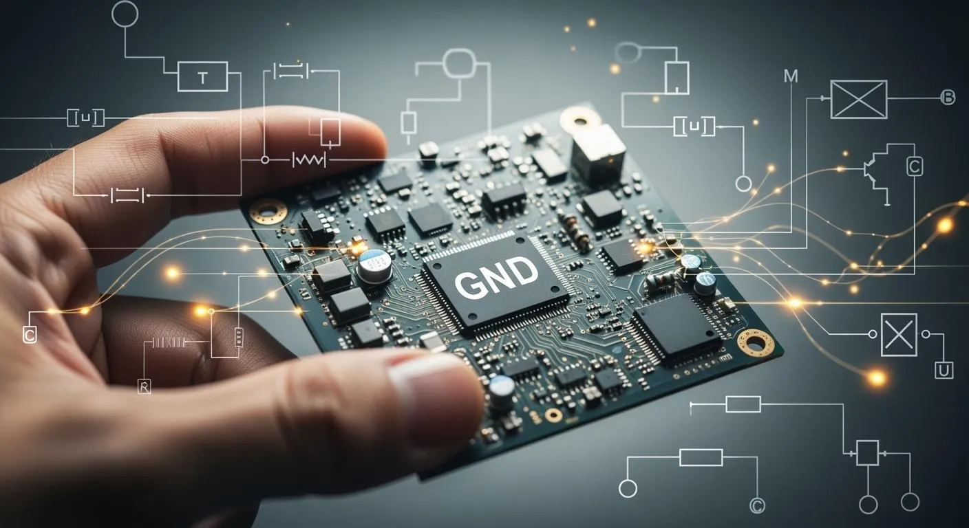
Three-Dimensional Integrated Circuits
Structure
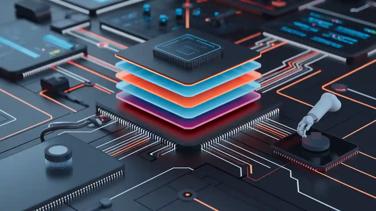
Three-dimensional integrated circuits stack many IC layers on top of each other. This makes the device smaller and helps it work better. Engineers use through-silicon vias to connect the layers. These vias let data move quickly between the stacked parts. Wafer bonding, like oxide and hybrid bonding, helps line up and join the layers. Interposer technology connects chiplets next to each other or in stacks. This helps keep the device cool and makes signals faster.
-
3D ICs put two or more chiplets on top of each other or on interposers with special packaging.
-
The design breaks big chips into smaller chiplets, like logic, memory, or sensors, and stacks them to help them talk to each other more.
-
Hybrid bonding makes strong connections between the stacked chiplets.
-
3D ICs work better, use less power, save space, and stay cooler.
|
Engineering Benefit |
Explanation |
|
|---|---|---|
|
Stacking layers up and down |
Shorter connections |
Shorter wires use less power and make signals faster. |
|
Shorter connections |
Less power needed |
Smaller wires waste less energy, which is good for tiny chips. |
|
Shorter wires |
Faster signals |
Lower RC time means signals switch faster and don’t slow down. |
|
Stacking analog and digital blocks |
Better signals |
Keeping parts apart stops noise and crosstalk. |
|
Stacking layers |
Saves space |
Smaller and thinner chips fit more parts in one place. |
|
Special technologies |
TSVs, wafer bonding, interposers |
These help connect layers and keep the structure strong. |
Three-dimensional integrated circuits use tiny imaging tools, like X-ray computed tomography, to look inside. This lets engineers see inside without breaking the IC. The design lets 3D ICs have lots of transistors and work well, even on bendy surfaces.
Heterogeneous Integration
Heterogeneous integration in 3D ICs puts different microelectronics, like logic, memory, sensors, and application-specific integrated circuits, together in one small package. Each chiplet can use the best process for its job. Designers can stack chiplets made from different materials and with different uses. This makes the system flexible and strong.
3D ICs use stacking and interposers to link chiplets. This makes the wires shorter and lets them talk faster. The design lets analog and digital parts work together without making the chip bigger. Engineers use new microelectronics and semiconductor processes to make sure the chips work well and last long.
Note: Heterogeneous integration in three-dimensional integrated circuits lets engineers build new systems for microelectronics, cars, and healthcare.
The design of 3D ICs keeps getting better. Engineers want to make the design stronger, fix heat problems, and fit more parts in. The future of three-dimensional integrated circuits depends on better semiconductor technology and microelectronics design.
3D IC Technology
Near-Sensor Computing
3d ic technology has changed how engineers work with near-sensor computing. Stacking chips on top of each other puts the processor close to the sensor. This means signals do not have to travel far. Devices work faster and use less energy. Engineers use 3d ic technology to let sensors process data right away. This helps devices react quickly and saves power.
Researchers made pressure sensors inspired by starfish using 3d ic technology. These sensors can feel many different pressures, like human skin does. They use hourglass-shaped parts to make them more sensitive. In tests, memristor-sensor arrays help cut down on noise. Monolithic 3d ic technology lets analog RRAM-based computing-in-memory work with sensors. This makes near-sensor computing use less energy. Some systems use as little as 140 pJ, which is almost as good as living things.
|
Metric/Feature |
Description/Value |
|---|---|
|
Energy Consumption |
As low as 140 pJ, similar to biological systems |
|
Sensor Design |
Starfish-inspired, hourglass microstructures, high aspect ratio |
|
Sensitivity Range |
Broad, mimics human skin |
|
Integration Approach |
Monolithic 3d integration of analog RRAM-based computing-in-memory with sensors |
|
Functional Roles |
Artificial nociceptor, tactile near-sensor computing unit |
3d ic technology lets smart sensors grow and stay small. Adding more sensors and processors does not make the device big. This is why 3d ic technology is great for IoT and wearable gadgets.
Emerging Materials
Material science is helping 3d ic technology get better. Scientists use very pure silicon and special semiconductors like gallium nitride. These help make devices smaller and work better. New nanomaterials, like graphene and transition metal dichalcogenides, make devices conduct electricity well and bend easily. Wide-bandgap semiconductors, such as silicon carbide, help devices handle more power and last longer.
Engineers use copper hybrid bonding to stack chips in 3d ic technology. Copper makes strong connections and helps keep things cool. This is important for good performance and longer device life. New chip designs, like gate-all-around and nanosheet transistors, help devices get smaller and work better.
Recent studies look at two-dimensional semiconductors, carbon nanotubes, and fast-moving polymers. These materials let engineers try new ways to design 3d ic technology. Spin-based MRAM and new device types that use electron spin or light open up new ways to store and use data. Material engineering helps devices handle more power and last longer, which is important for the future of 3d ic technology.
Note: Using new materials and smart designs keeps 3d ic technology leading smart sensing research.
Benefits of 3D ICs
Three-dimensional integrated circuits give smart sensing many big benefits. These ics help make sensors smaller and more efficient. They also let more parts fit into one device. Devices get smaller, use less power, and work better. Engineers notice less signal delay and better power use. Systems can also change more easily.
Miniaturization
3d ics help engineers make devices much smaller. Stacking ic layers saves space on the wafer. Three-dimensional connections on III-V semiconductor heterostructures use wafer space six times better than two-dimensional ones. Device sizes can get up to a thousand times smaller. This means tiny sensors can go in wearables, medical tools, and electronics.
HiSilicon Solutions in Miniaturization
HiSilicon uses 3d ic stacking for phones, wearables, and IoT gadgets. Their chips make products take up less space. These ics keep things light and small but still have smart sensing.
Performance
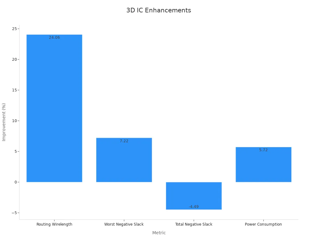
3d ics make devices work better by making connections shorter. Stacking layers up and down cuts wire length by about 25% compared to 2d designs. This makes data move faster and saves energy. Devices can process information quickly and use less power. The table below shows important performance numbers:
|
Metric/Comparison |
Description/Result |
|---|---|
|
Routing Wirelength (rWL) |
3d methods improve wire length by about 25% over 2d; average is 24.06% better because of vertical connections and mem-on-logic design. |
|
Power Consumption |
3d ics use 5.72% less power than 2d, and 3d-DMP is 1.98% better than 3d-Tiling. |
|
Thermal Simulation |
3d ics can get hotter because they pack more parts together. |
HiSilicon Solutions in Performance
HiSilicon’s smart vision chips and media parts use 3d ic technology. These chips have less signal delay and faster data speeds. Devices can do real-time video and AI with less power.
Integration Density
3d ics stack many layers to fit more parts in one place. This makes wires 30% to 50% shorter when using 2-4 layers. Monolithic inter-tier vias (MIVs) add even more connections and cut the longest path delay by up to 33%. Power used by wires between blocks drops by up to 35%. The table below shows these gains:
|
Metric |
3D IC Improvement |
Details |
|---|---|---|
|
Wire length reduction |
30%-50% |
For 2-4 device layers, compared to 2d ics. |
|
Via density |
Higher for MIVs |
Lets devices have many more vias. |
|
Longest path delay reduction |
Up to 33% |
MIV-based 3d ics. |
|
Inter-block net power reduction |
Up to 35% |
MIV-based 3d ics. |
HiSilicon Solutions in Integration Density
HiSilicon’s optical modules, A2 MCUs/MPUs, and analog chips use 3d ic integration. These products put many subsystems in one small package. Devices get better power use, more flexibility, and higher performance.
Applications
IoT
The Internet of Things uses 3d ic technology to make smart sensors. These sensors mix MEMS and CMOS electronics in one package. Teams for digital, analog, RF, and MEMS work together on the design. They start with flat mask layouts and then build 3d MEMS models. These sensors help in real-world jobs like checking building health. For example, IoT devices with 3d sensing give live 3d acceleration data. Servers use this data to show how buildings move. People can see these results as a 3d model in a web browser. Companies like Arm and Intel make dense 3d logic chips for IoT. Shorter signal paths cut power use by up to 100 times. Modular stacking lets people make custom IoT designs.
-
3d NAND memory stacks help make IoT devices smaller.
-
Wide bandwidth buses make IoT systems work better.
-
Shorter wires, by 10–15%, save power.
Automotive
Cars use 3d ic technology in many ways. New cars have smart sensors for safety and driving help. 3d integration lets car makers add more features in less space. Sensors check tire pressure, engine health, and how drivers act. ADAS uses 3d ic sensors to process data fast. This helps with lane-keeping, crash avoidance, and cruise control. The car industry uses 3d tech to meet tough safety rules.
Healthcare
Healthcare uses 3d ic technology to make strong, flexible sensors. Engineers made wearable patches with 3d micro strain gauges. These patches measure force and skin temperature. The sensors link to wireless circuits on bendy boards. Patients wear these patches for constant checks during therapy. 3d ic integration makes small medical devices with memory, sensors, and processors. Hospitals use these for checking, finding, and treating health problems. Some implants send patient data to doctors far away. In clinics, 3d ic chips help find diseases like age-related macular degeneration quickly and accurately.
Consumer Electronics
Consumer electronics use 3d ic technology for fast, energy-saving devices. The market for 3d ic in this area is growing quickly. In 2024, the market was about $5.99 billion. Experts think it will grow 20% each year. By 2034, the market could reach $33.7 billion.
|
Attribute |
Consumer Electronics |
|---|---|
|
Market Size (2024 Estimate) |
About US$ 5.99 Billion |
|
Compound Annual Growth Rate (2024-2034) |
20% CAGR |
|
Projected Market Size (2034 Forecast) |
About US$ 33.7 Billion |
Phones, tablets, and wearables use 3d ic stacks for better speed and longer battery life. People want small, powerful devices, so 3d tech is used more. Semiconductor sales reached $49.1 billion in May 2024. This shows a big need for advanced 3d ic parts in consumer products.
Challenges
Manufacturing
Making three-dimensional integrated circuits is hard for engineers and companies. They must stack layers, make through-silicon vias, and use careful bonding. Each step makes things harder and riskier. Sometimes, tools break or the process changes, which causes problems. If a wafer has 260 dies and 18 are bad, the yield is 93%. Even small problems can lower how many good chips they get. Engineers spend lots of time looking for where things go wrong. They need to know a lot to fix many problems on one wafer.
-
Special tools and materials make manufacturing expensive.
-
Yield management finds and fixes defects in stacked dies and TSVs.
-
Machine learning helps find problems, sort defects, and improve designs.
Note: AI and ML now help spot problems, guess what will happen, and keep machines working well, so making chips is easier.
Thermal Management
Keeping three-dimensional integrated circuits cool is a big problem. Stacked layers make more heat in a small space. This raises the temperature and makes hot spots, especially in the middle. High thermal resistance slows down how fast heat moves out. Uneven heat can stress the chip and cause it to bend or break.
|
Thermal Challenge |
Impact on 3D ICs |
|---|---|
|
High thermal resistance |
Makes it hard for heat to leave, so chips get hotter |
|
Hotspots and gradients |
Can hurt how well chips work and last |
|
Thermal stress-induced deformation |
Can bend or damage the chip |
|
Non-uniform temperature |
Makes cooling and keeping chips stable harder |
Engineers use computer tools to see how heat moves and try new ways to cool chips. Diamond heat sinks and tiny channels help lower the hottest spots and stress. Better designs move heat faster and help chips last longer.
Cost
Cost is still a big problem for companies that want to use three-dimensional integrated circuits. Making these chips costs more because stacking, TSVs, and bonding are hard. If there are more bad chips, companies lose money. High costs for making and designing slow down how fast people use these chips.
-
Special machines and materials cost more money.
-
More steps mean more work and time.
-
Better ways to make chips and design them can lower costs.
-
Good cooling and stronger chips save money over time.
Companies keep working on new ways to make three-dimensional integrated circuits cheaper and better for smart sensing in the future.
Innovations
Packaging
Engineers have made new ways to package three-dimensional integrated circuits. These new ways help devices work better and cost less money. The table below lists some top packaging solutions and what they do:
|
Packaging Solution |
Key Features |
Technical Evidence |
Application Areas |
|---|---|---|---|
|
FOCoS (Fan-Out Chip-on-Substrate) |
Multi-layer RDL, fine lines, large module size, replaces TSV interposer |
Better electrical performance, lower cost, high-volume production, supports chiplet integration |
HPC, AI/ML, Networking, Cloud |
|
FOSiP (Fan-Out System-in-Package) |
System-level integration, miniaturization |
Enables highly integrated systems, reduces component size, improves performance |
Mobile, Telecom, Consumer Electronics |
|
FCPoP (Flip-Chip Package-on-Package) |
Thin, light, low-inductance interconnects |
Used in mobile devices, supports HD display, low power |
Smartphones, Tablets, Wearables |
|
2.5D/3D Integration Platforms |
Silicon interposer, CTE matched substrates |
High interconnect density, low latency, reduces failure |
HPC, Networking, Graphics |
These packaging methods are used in real products today. They help companies make smaller, faster, and more reliable smart sensing devices.
Cooling Solutions
Three-dimensional integrated circuits need good cooling to work well. Stacked layers make more heat in a small space. Engineers look at different cooling ways to see which is best:
|
Cooling Method |
Heat Dissipation Efficiency |
Limitations |
|---|---|---|
|
Air Cooling |
Low |
Needs large area, not enough for 3D ICs |
|
Static Heat Sink |
Moderate |
Limited heat transfer inside stacked dies |
|
TSV Cooling |
Moderate |
Needs special placement, still needs extra cooling |
|
High |
Needs special microchannel patterns |
Microfluidic cooling works the best out of all the choices. It uses tiny channels to move liquid through the chip. This cools down hot spots and lowers the chip’s temperature. It spreads heat evenly and cuts pumping power by 37.5%. The chart below shows how each cooling method works:
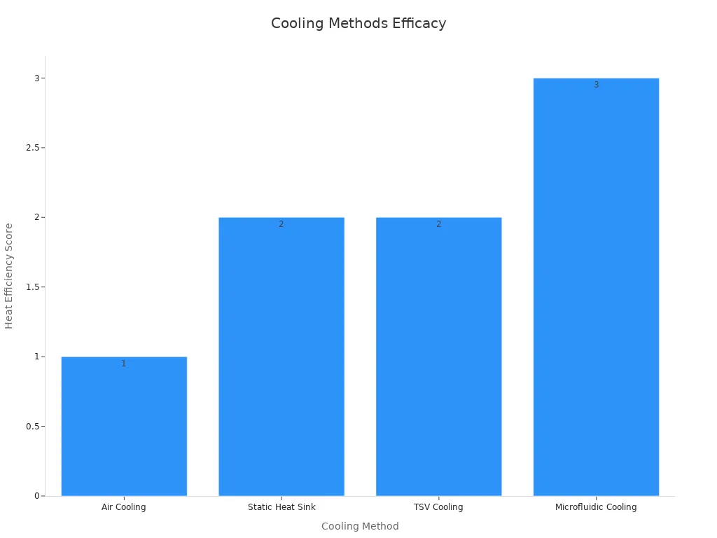
Microfluidic cooling fits well with how 3D ICs are made. It helps chips last longer and work better, so it is a top pick for smart sensing.
Cost Reduction
Companies want to make three-dimensional integrated circuits cheaper. They use new packaging and cooling to save money. FOCoS and FOSiP packaging mean companies do not need expensive silicon interposers. Microfluidic cooling helps chips last longer, which saves money over time. Using machines and better ways to check for mistakes also lowers costs. These steps help smart sensing technology grow and spread.
Market Trends
Growth
The market for three-dimensional integrated circuits is growing fast. In 2024, it was worth $12.41 billion. Experts think it will be $14.41 billion in 2025. The yearly growth rate is 16.1%. By 2029, it could reach $25.83 billion. This fast growth happens because people want better electronics. They also want devices that save energy and work well. Consumer electronics, cars, healthcare, IoT, and AI help the market grow. In 2024, the global market was $16.4 billion. It may reach $49.66 billion by 2033. The semiconductor industry uses vertical stacking and through-silicon via interconnects. These make devices work better and use less power. The market also grows with better packaging, new materials, and improved ways to make things. Sensors will have 31.7% of the market in 2025. Consumer electronics will have 38.6%. This shows that smart gadgets help the market grow.
Industry Leaders
Some companies are the top players in this market. They spend money on research to stay ahead. They try to make devices smaller, faster, and more reliable. Intel, TSMC, Samsung, and HiSilicon are important companies. They use new ways to package and stack chips. Their products help smart sensing in many areas. These companies also help set rules for the market. Their new ideas help the market grow and affect other companies.
Regional Adoption
Asia Pacific is the leader in this market. China’s market could be $2.2 billion by 2033. Japan’s market could be $1.9 billion. Both countries want small electronics because space is limited. The United States could have a market worth $8.2 billion by 2033. The US market grows because of data and security needs. Consumer electronics in these places grow at 8.1% each year. IoT, AI, and 5G help this trend. The semiconductor industry in these areas tries new ideas to meet demand. Local needs in each region help shape the world market.
Note: The market for three-dimensional integrated circuits will keep growing as the semiconductor industry changes with new trends and technology.
Future Outlook
Advancements
The future for three-dimensional integrated circuits in smart sensing looks bright. Big companies have plans that show steady progress in 3D integration. Through Silicon Vias, vertical packaging, and monolithic 3D integration will help make new devices. The Frost & Sullivan Integrated Technology Roadmap says these changes will affect many areas. Smart sensing, consumer electronics, and aerospace will get the most benefits. The roadmap also talks about new business ideas and changes in the companies that make chips.
Scientists and engineers keep working on new ideas. They want to make things smaller, use less power, and work better. These goals fit what the smart sensing market needs. The Persistence Market Research report says the 3D IC and 2.5D IC market will grow from $62.1 billion in 2025 to $111.3 billion by 2032. This shows people want better packaging and new uses. 3D TSV packaging will be a big part of the market by 2032. Research teams look for new materials and smarter designs to fix cost and process problems. Because of this, the chip industry will have better and stronger solutions in the future.
Industry Impact
These new changes will help many industries. The market for 3D ICs will grow in electronics, phones, cars, and medical devices. Smart sensing will be used more in everyday life. Devices will get smaller, faster, and use less energy. The chip industry will find new chances as more companies use 3D integration.
Companies that spend money on research will lead the market. They will start new trends and help shape the future of smart sensing. There will be more teamwork and new ways to make and sell products. As the market gets bigger, the chip industry will need to keep up with new needs and technology.
A table below shows the main areas that will change:
|
Sector |
Expected Impact in the Future |
|---|---|
|
Consumer Electronics |
Smaller, smarter devices |
|
Automotive |
Safer, more reliable systems |
|
Medical Devices |
Better, real-time health monitoring |
|
Telecommunications |
Faster, more efficient networks |
The future will bring more research, new products, and a stronger market for three-dimensional integrated circuits. The chip industry will keep changing to meet the needs of smart sensing and more.
Three-dimensional integrated circuits have changed smart sensing a lot. Devices are now smaller, quicker, and use less energy. But there are still some big problems to fix. Companies need to solve issues with making, cooling, and cost.
-
Put money into making both 2.5D and 3D chips in new ways.
-
Use different places to get materials so there are fewer supply problems.
-
Work with others to make better ways to connect and pack chips.
-
Spend time and money on research to cool chips better.
If people keep coming up with new ideas and work together, this area will keep growing.
FAQ
What makes three-dimensional integrated circuits important for smart sensors?
Three-dimensional integrated circuits help smart sensors get smaller and work faster. Engineers can put more parts into one device by stacking them. This makes the device work better and use less power.
How do 3D ICs improve energy efficiency in devices?
3D ICs make signals travel a shorter distance inside the chip. Shorter wires mean the chip uses less energy. Devices with 3D ICs can last longer on the same battery.
Are there any risks with using 3D ICs in smart sensing applications?
Engineers have problems with heat and cost. Stacked layers can get hot fast. Making these chips is also more expensive. Companies are trying new ways to cool and pack the chips to fix these issues.
Which industries benefit most from 3D IC technology?
Consumer electronics, automotive, healthcare, and IoT get the most help. Devices in these areas become smaller, smarter, and more reliable with 3D ICs.