Step-by-Step Guide to the Assembly of PCB for Electronic Product Prototypes
Printed Circuit Board (PCB) assembly is key to making electronic prototypes. It turns your ideas into working devices, connecting plans to real products. If assembly is done wrong, prototypes might not work or grow well.
Printed Circuit Board (PCB) assembly is key to making electronic prototypes. It turns your ideas into working devices, connecting plans to real products. If assembly is done wrong, prototypes might not work or grow well.
This Step-by-Step Guide for PCB assembly ensures that every part, like picking materials, preparing them, testing, and checking quality, contributes to building a strong and useful product. This guide will show you how to do it right so your prototypes match your design and work as expected.
Key Takeaways
-
A good PCB design is key for working prototypes. Check your design often to find problems early and save time.
-
Pick the right materials for your PCB to make it last. Strong materials like Rogers 4350 work well in tough conditions.
-
Use Surface Mount Technology (SMT) and Through-Hole Technology (THT) as needed. SMT is great for small gadgets, while THT is strong for heavy-duty uses.
-
Test your PCB carefully with tools like Automated Optical Inspection (AOI) and functional tests. This helps you fix issues before making more.
-
Talk clearly with your manufacturer and follow rules to keep quality high during large-scale production.
Step-by-Step Guide to PCB Design and Prototyping
Importance of a well-thought-out PCB design
A good PCB design is key for successful electronic prototypes. It helps your product work well and meet design goals. Using a clear process can lower mistakes and save time.
-
Iterative Improvement: Check your design often to find problems early. This avoids wasting time and money during production.
-
Design for Manufacturability (DFM): Follow simple rules to make your design easier to build. This reduces errors and keeps production smooth.
-
Quality Control: Test your design carefully to find issues before moving forward.
A smart design also boosts how your product works. For example, fast designs improve signal flow, while HDI designs save space without losing features. Special PCB technologies, like rigid-flex or metal-core PCBs, make products stronger in tough conditions.
|
Strategy |
Description |
|---|---|
|
Helps signals move reliably by planning paths carefully. |
|
|
Space constraints addressed |
Uses HDI designs to fit tight spaces without losing quality. |
|
Specialist PCB technologies |
Adds rigid-flex or metal-core PCBs for strength in harsh places. |
Tools and software for creating schematics and layouts
Picking the right tools for PCB design is important to turn ideas into working prototypes. Design software helps with schematics, layouts, and testing.
|
Software |
Key Features |
Best For |
|
|---|---|---|---|
|
Altium Designer |
Advanced routing, 3D visualization |
Professionals |
4.5/5 |
|
Cadence Allegro |
Robust simulation, collaboration |
High-performance projects |
4.6/5 |
|
Mentor Graphics Xpedition |
High-speed design, analysis |
Large teams |
4.4/5 |
|
OrCAD PCB Designer |
User-friendly, strong libraries |
Beginners |
4.3/5 |
|
KiCAD |
Free, full design suite |
Hobbyists |
4.6/5 |
Beginners can try EasyEDA or Fritzing for simple tools. Experts might choose Altium Designer or Cadence Allegro for advanced options.
Translating concepts into functional designs
Turning ideas into working designs takes several steps. Start by drawing your idea and making 3D CAD models. Use DFM rules to keep designs practical.
Then, create a PCB with parts like sensors, wireless systems, and power controls. Build prototypes to test and improve your design based on results.
|
Stage |
Description |
|---|---|
|
Turned sketches into 3D CAD models using DFM rules. |
|
|
PCB Design |
Made a PCB with sensors, wireless systems, and power controls. |
|
Prototyping |
Built prototypes, starting with 3D-printed models for testing. |
|
Final Optimization |
Improved design after testing to meet all needs. |
|
Market Readiness |
Prepared the prototype for production and market launch. |
Following these steps will help you create a strong and reliable product.
Material Selection in the PCB Assembly Process
Picking the right PCB substrate for prototypes
Choosing the correct substrate is very important for making prototypes. The substrate affects how well your PCB works in different situations. Materials like FR4, 370HR, and Rogers 4350 have different levels of heat stability, electrical properties, and costs.
|
Material |
Dissipation Factor (Df) |
Coefficient of Thermal Expansion (CTE) |
|
|---|---|---|---|
|
FR4 |
4.0 – 4.5 |
0.02 – 0.03 |
14 – 16 ppm/°C |
|
370HR |
3.5 – 3.9 |
0.015 – 0.025 |
13 – 15 ppm/°C |
|
Rogers 4350 |
3.48 |
0.0037 |
13 ppm/°C |
|
Taconic TLY-5 |
3.55 |
0.0025 |
15 ppm/°C |
|
Metal Core |
Varies |
Varies |
Varies |
When picking a substrate, think about its decomposition temperature (Td) and glass transition temperature (Tg). Materials with high Td work better in lead-free environments and during repeated heating. This helps make the PCB more reliable.
Tip: For strong prototypes, use substrates like Rogers 4350 or Taconic TLY-5. These materials are great for heat stability and signal quality.
Choosing components based on cost and function
Balancing cost and function is key when picking parts for prototypes. You should check parts for their features, compatibility, and how they are made.
-
Look at features to ensure good performance.
-
Use new technologies to improve your design.
-
Make sure parts work well together.
-
Study other products for ideas.
-
Pick manufacturing methods that lower costs.
-
Use EDA tools to test your design.
-
Choose parts that work for mass production.
-
Find a balance between cost and performance.
By following these steps, you can pick parts that fit your design without spending too much. This keeps the PCB assembly process smooth and affordable.
Checking material quality for reliable assembly
Good material quality makes prototypes more reliable. Testing methods like Automated Optical Inspection (AOI) and X-ray checks help find problems early. Functional tests make sure the PCB works as needed.
|
Quality Control Metric |
Description |
|---|---|
|
Automated Optical Inspection (AOI) |
Finds mistakes in assembly. |
|
X-ray Inspection |
Checks hidden solder connections. |
|
Functional Testing |
Makes sure the board works correctly. |
|
Manual Inspection |
Looks for any leftover issues. |
|
Compliance with Industry Certifications |
Like ISO 9001, AS9100, and IPC standards. |
Using good materials and strong testing methods ensures your PCB prototypes are reliable.
Note: Always choose materials that meet industry certifications for long-lasting reliability.
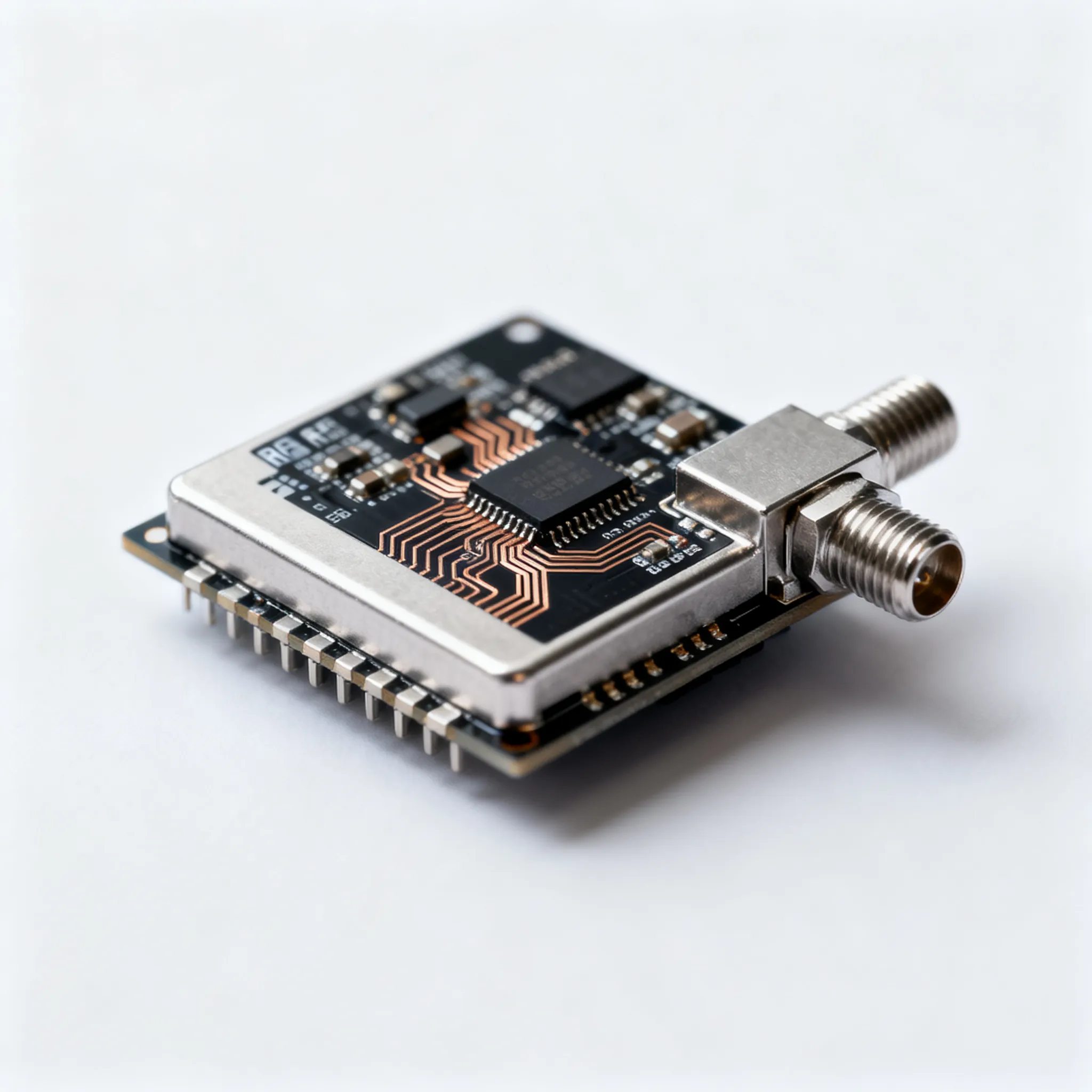
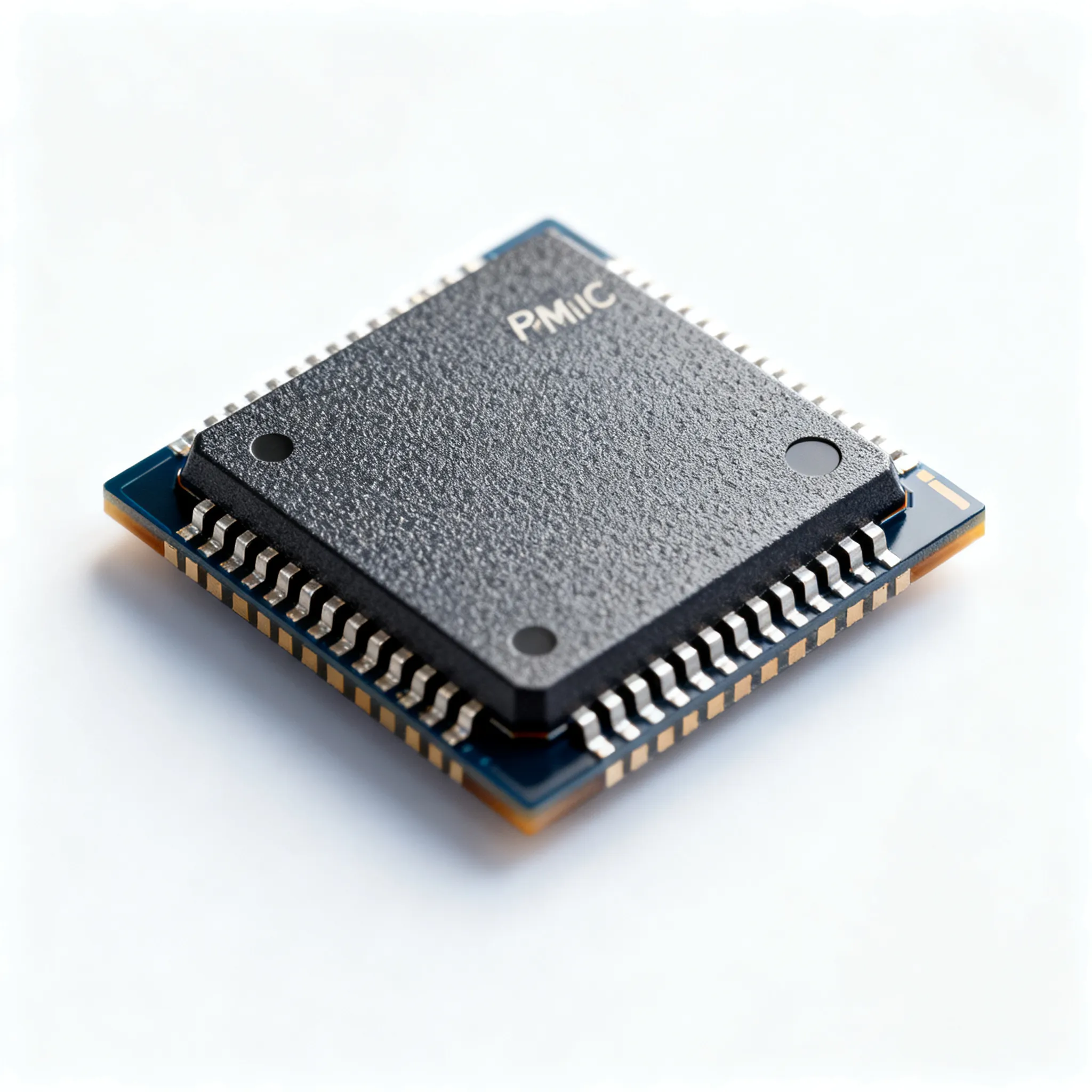
PCB Production and Assembly: Fabrication Process
Steps involved in PCB manufacturing
Making a PCB involves many steps to turn designs into boards. First, raw materials like the substrate and copper layers are prepared. Then, a photoresist coating is added, and UV light transfers the design onto the board. Etching removes extra copper, leaving only the needed traces and pads.
Next, holes are drilled for parts and vias. These holes are plated with conductive material to allow electricity to flow. Solder masks protect the board, and silkscreens label the parts. Finally, the board is cut and tested to ensure it works as planned.
Common fabrication methods and their applications
Different methods are used for making PCBs based on their purpose. Simple single-sided or double-sided boards are good for prototypes because they cost less. Multilayer boards are better for complex designs like medical or telecom devices.
Flexible PCBs are great for wearable gadgets. Rigid-flex boards combine strength and flexibility for cars or airplanes. Metal-core boards handle heat well, making them ideal for LED lights or power systems.
Each method has its own advantages. Pick the one that fits your design and product needs.
Ensuring precision during fabrication
Accuracy is very important when making PCBs to avoid mistakes. Clear communication with the manufacturing team helps everyone follow the same rules. IPC standards, like IPC-A-600 for looks and IPC-6012 for strength, guide the process.
Team consistency reduces errors and improves quality. IPC-A-610 explains soldering and cleaning, while IPC-2221 shares tips for materials and layouts. Following these rules ensures your PCB meets industry standards and works well.
Tip: Check if your manufacturer follows IPC standards. This ensures good quality and fewer problems.
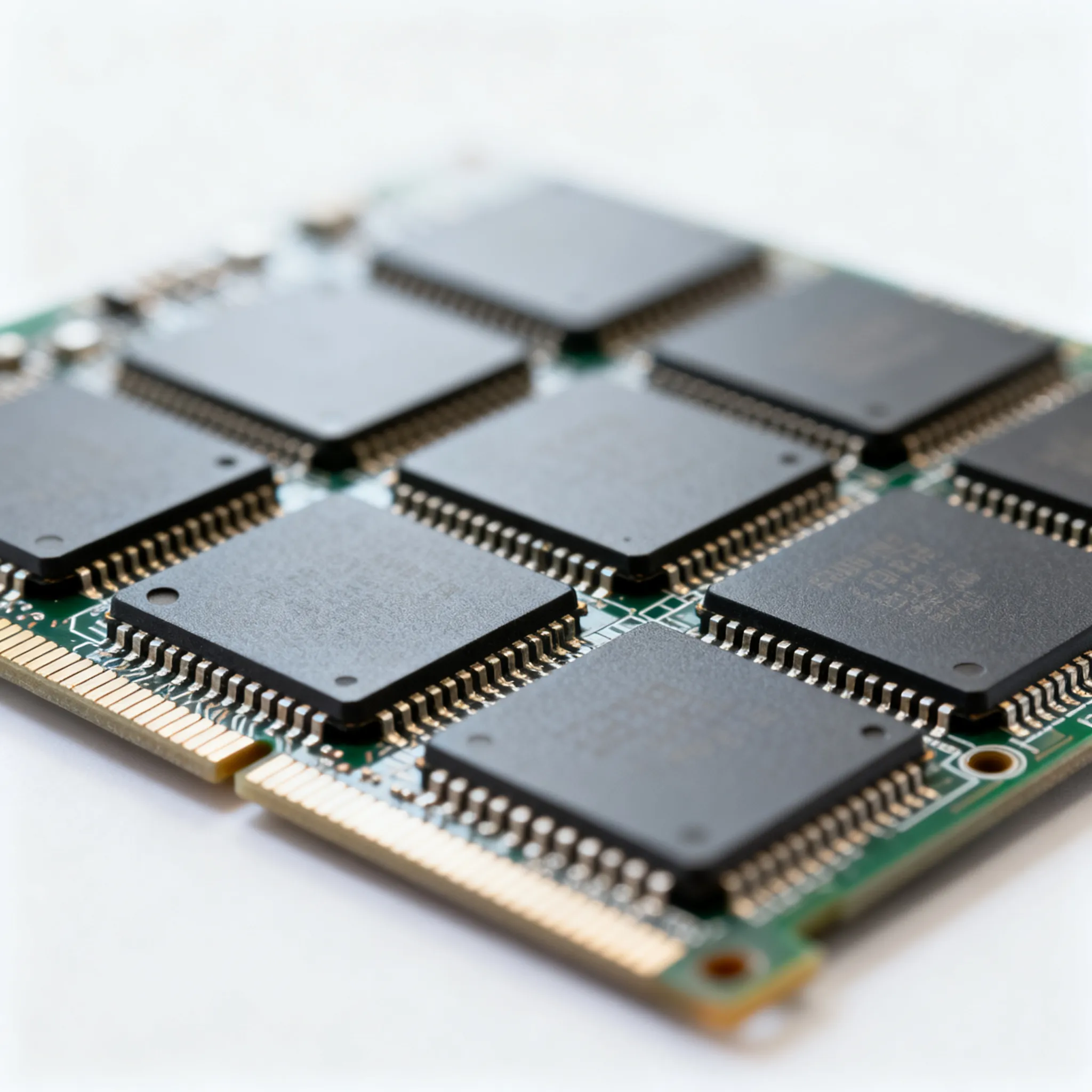
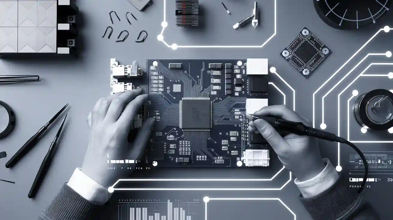
Component Mounting Techniques in PCB Assembly
Surface Mount Technology (SMT) overview
Surface Mount Technology (SMT) is a modern way to attach parts directly to a PCB. It is popular because it works fast and fits many parts in small spaces.
SMT skips drilling holes, making designs smaller and lighter. Machines place parts automatically, which is quicker and more accurate than doing it by hand.
Main benefits of SMT:
-
High efficiency: Machines speed up the assembly process.
-
Cost-effectiveness: Cheaper for making many products.
-
Compact designs: Parts are closer together, saving space.
To check SMT PCBs, manufacturers use advanced tests:
-
Automated Optical Inspection (AOI) finds mistakes in tight layouts.
-
X-ray testing checks hidden connections.
-
In-circuit testing ensures parts work before production finishes.
SMT is common in gadgets like phones and laptops, where small size and good performance matter.
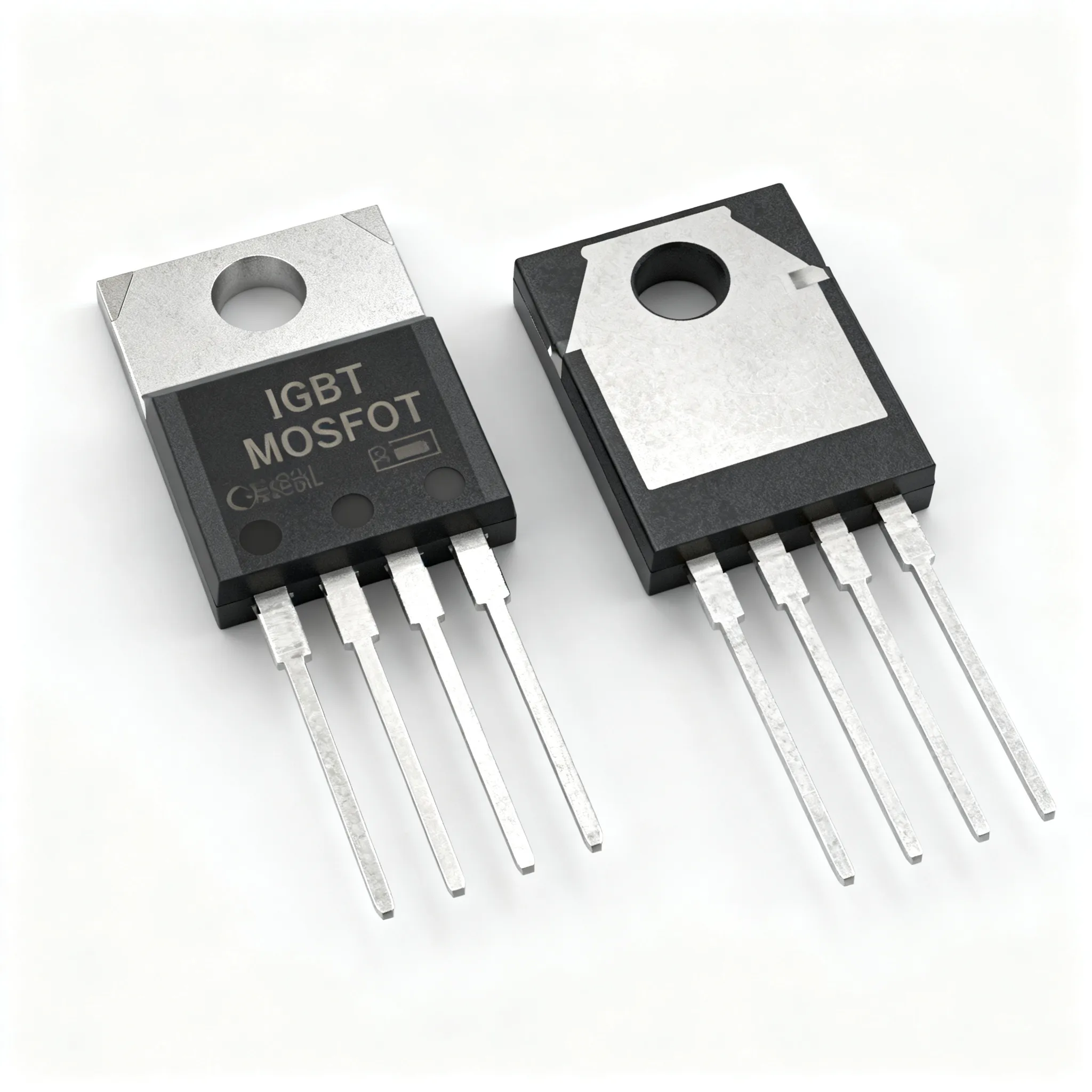
Through-Hole Technology (THT) overview
Through-Hole Technology (THT) is an older method where parts go through holes in the PCB. The leads are soldered on the other side to hold them in place.
THT makes strong connections, so it’s great for tough products. But it takes more time and costs more than SMT.
THT advantages:
-
Durability: Stronger connections for tough environments.
-
Ease of prototyping: Simple for small projects and testing.
THT downsides:
-
Drilling holes leaves less space for circuits.
-
Manual soldering takes longer and costs more.
THT is used in cars, planes, and factories where strength and power are important.
Comparing SMT and THT: Applications and advantages
SMT and THT each have their own strengths. Picking the right one depends on your project needs.
|
Advantages |
Disadvantages |
|
|---|---|---|
|
Through-Hole Assembly |
Stronger connections, good for reliable products. |
Slower, more expensive, less space for circuits. |
|
Surface Mount Assembly |
Faster, cheaper, fits more parts in small spaces. |
Less reliable for parts that face physical stress. |
Where SMT works best:
-
Phones, small gadgets, and fast circuits need SMT for its size and speed.
-
SMT fits more parts into smaller designs.
Where THT works best:
-
Cars, planes, and factory machines need THT for strength and power.
-
THT is easier for testing and small projects.
Cost differences:
-
SMT is cheaper for big batches because machines do the work.
-
THT costs more due to drilling and hand soldering.
Using both SMT and THT can improve your PCB. For example, use SMT for small parts and THT for strong connectors.
Tip: Use SMT for large production and THT for strong, durable prototypes.
Soldering and PCB Assembly Process
Important tools for soldering
Using the right tools makes soldering easier and more accurate. These tools help you work faster and ensure good results.
-
Soldering Iron or Station: Heats solder for joining parts. Adjustable heat settings improve control.
-
Solder Wire: Common types are SAC305 and SnPb. Pick based on your project needs.
-
Flux: Helps solder flow better and stops oxidation. Types include no-clean, water-soluble, and rosin-based.
-
Desoldering Tools: Fix mistakes by removing extra solder. Use tools like solder wick or vacuum pumps.
-
Magnifying Glass or Microscope: Lets you see tiny parts and solder joints clearly.
-
Automated Systems: Machines like solder pots and fluxing units apply solder precisely.
Tip: Use AOI and X-ray checks to confirm solder joints are good.
Tips for soldering components
Good soldering practices make assembly easier and reduce mistakes.
-
Keep your workspace clean and tidy to avoid problems.
-
Group similar parts together to prevent mix-ups.
-
Place important parts close to power sources. Use short paths for capacitors.
-
Arrange power supply parts near the power input.
-
Leave enough space for machines to work properly.
-
Follow heating and cooling rules to protect parts from damage.
-
Check solder joints with your eyes or AOI systems to ensure they are strong.
Note: Studies show HASL finishes make solder joints stronger than OSP. Picking the right finish improves assembly quality.
How to avoid soldering mistakes
Mistakes during soldering can cause your PCB to fail. Follow these tips to avoid common errors:
-
Don’t overheat parts. Too much heat can ruin them.
-
Avoid cold solder joints. Make sure solder melts fully and sticks well.
-
Use the right amount of solder. Too much causes bridges; too little makes weak joints.
-
Keep tools clean to avoid adding dirt to the assembly.
-
Fix bad solder joints quickly. Follow customer rules for repairs or replacements.
-
Clean the board before adding coatings. Dirt can stop coatings from sticking.
Tip: Inspect solder joints before finishing the assembly. This step ensures quality and lowers the chance of failure.
Inspection and Testing in PCB Assembly
Visual inspection for assembly errors
Visual checks are the first step to ensure your PCB is good. They help find surface problems and mistakes before deeper tests. Use tools like magnifying glasses or microscopes to spot issues. Look for solder bridges, crooked parts, or broken traces.
Automated Optical Inspection (AOI) makes this process faster. It scans the PCB right after soldering to find missing or misplaced parts. AOI uses cameras and smart software to catch errors quickly. This method works well in production lines and reduces fixing time.
Tip: Use both manual checks and AOI for better results. This helps find visible and hidden problems in your PCB.
Functional testing methods for prototypes
Functional tests check if your PCB works as planned. They mimic real-world use to test how the board performs. Simple power-on tests can confirm basic functions like voltage output. For complex designs, program firmware and test all parts to ensure they work.
Automated tests use special tools and software to simulate real conditions. These tests are quick and give detailed results about the board’s performance. Debugging during tests involves checking power signals, isolating sections, and using indicators to find problems.
Functional testing steps include:
-
Running the board in real-world-like conditions.
-
Checking basic functions with power-on tests.
-
Testing all parts for full checks.
-
Using automated tools for faster and accurate results.
Note: Functional tests are key for final checks. They make sure your PCB meets design needs and works reliably.
Debugging and troubleshooting techniques
Debugging finds and fixes problems in your PCB. Start by checking power and clock signals, as they are important for the board to work. Use indicator signals to monitor parts and sections.
Testing one section at a time helps find where the issue is. Tools like oscilloscopes and logic analyzers show signal details to help solve problems.
Common debugging steps include:
-
Checking power connections.
-
Looking for short circuits or broken paths.
-
Testing each part for faults.
-
Using tools to check signal quality.
Tip: Write down your debugging steps to make future fixes easier. This saves time and keeps your testing process organized.
Transitioning from PCB Prototype to Mass Production
Scaling up PCB production efficiently
Making more PCBs needs good planning for quality and speed. Pick strong materials like durable substrates and finishes for long-term use. Follow DFM rules to make layouts better, avoid mistakes, and increase success rates. Check the process for repeatable results in trace sizes, layer placement, and drilling accuracy.
Make sure your design works well for large amounts without losing quality. Use standards like IPC Class 2 and Class 3 for reliable results. Work closely with your manufacturer to agree on details, quality checks, and schedules. This teamwork keeps costs low and prevents delays.
Tip: Write down each production step to keep track and find ways to improve.
Cost-effective strategies for mass production
Saving money in mass production needs smart planning. Use value engineering to study parts and find cheaper options. Standardizing parts makes assembly easier and cuts costs. For example, using fewer types of parts in your BOM reduces waste and speeds up production.
Machines can solder faster and cheaper than people. Automated soldering costs about $0.01 per joint, while manual soldering costs $0.05. Making more units lowers the cost per item. For example, producing 1,000 units instead of 100 can cut costs by 30-40%.
Note: Don’t rush production unless needed. A regular 10-day schedule costs less than a 48-hour rush, which can raise costs by 50%.
Ensuring design consistency during production
Keeping designs the same is important for mass production. Use tools like AOI and X-ray tests to find mistakes in assembly. Electrical tests check circuits, and peel tests confirm the board’s strength.
Work with your manufacturer to follow rules like IPC-A-600 for looks and IPC-6012 for performance. Test prototypes often to make sure designs stay consistent in every batch. This reduces errors and keeps quality high.
|
Test Type |
Purpose |
|---|---|
|
Visual and X-Ray Inspection |
Finds damage and checks inside connections for good solder joints. |
|
Electrical Tests |
Confirms circuits work and are properly isolated. |
|
AOI (Automated Optical Inspection) |
Spots assembly mistakes automatically, better than manual checks. |
Tip: Testing regularly during production ensures your PCBs meet standards and work well.
Using a clear process for PCB assembly makes sure your designs work well and meet quality needs. Testing at each step helps find mistakes early and improves how your prototype works. By following this guide, you can grow your designs easily and get them ready for large production. Use these methods to build strong and useful prototypes that match your plans.
FAQ
1. What is the key step in PCB assembly?
Testing is the most important step. It checks if your PCB works and meets design goals. Use tools like AOI and functional tests to find problems early.
2. Can SMT and THT be used on one PCB?
Yes, you can use both SMT and THT together. SMT is great for saving space, while THT adds strong connections. This mix gives both efficiency and durability.
3. How do I pick the right PCB material?
Choose a material based on your project’s needs. Think about heat resistance, signal quality, and cost. FR4 is a good all-around choice, while Rogers 4350 is better for high-frequency designs.
4. What tools are needed for soldering?
You’ll need a soldering iron, solder wire, flux, and tools to remove solder. A magnifying glass helps with small parts. Machines can make soldering faster and more accurate for big projects.
5. How do I prevent mistakes in PCB production?
Follow IPC rules and talk clearly with your manufacturer. Test your prototypes often and use tools like AOI to spot errors early.