Quality Testing Methods for Assembled PCB
Testing PCBs ensures they function properly and comply with regulations. You can utilize various Quality Testing Methods such as Visual Checks, In-Circuit Testing (ICT), Functional Testing, X-Ray Checks, Stress Testing, and Automated Optical Inspection (AOI).
Testing PCBs ensures they function properly and comply with regulations. You can utilize various Quality Testing Methods such as Visual Checks, In-Circuit Testing (ICT), Functional Testing, X-Ray Checks, Stress Testing, and Automated Optical Inspection (AOI). These Quality Testing Methods help identify issues early and enhance PCB quality. They also contribute to more consistent and reliable assembly. Effective PCB testing guarantees they operate without problems during normal use, which keeps customers satisfied. In today's assembly environment, robust Quality Testing Methods are essential to maintain steady quality. These methods safeguard the performance of your PCB and protect your brand's reputation.
Key Takeaways
-
Checking PCBs is important to make sure they work well.
-
Looking at them closely is a cheap way to spot problems.
-
In-Circuit Testing (ICT) is very good at finding mistakes fast.
-
Functional testing acts like real use to check if PCBs work right.
-
Using different tests helps find hidden problems and improves quality.
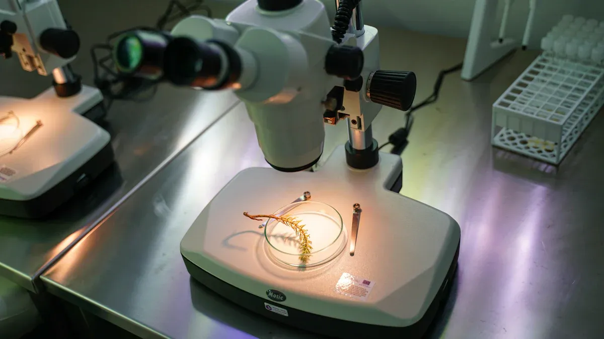
Visual Inspection
Purpose and Benefits
Visual inspection is important for checking PCB quality. It finds visible problems like bad soldering, missing parts, or misaligned pieces. This method is simple, cheap, and works well for small PCB batches.
Some main benefits of visual inspection are:
-
Skilled inspectors can quickly find visible problems, like soldering mistakes.
-
It is an affordable option for small-scale production quality checks.
But, this method has some downsides. Manual checks depend on the inspector's skill and focus. Tiredness or lack of experience can cause mistakes. Also, it cannot find hidden problems that can't be seen.
|
Benefit/Limitations |
Description |
|---|---|
|
Simplicity |
Visual inspection is easy to do and understand. |
|
Cost-effectiveness |
It is a cheap method for small PCB batches. |
|
Identifying visible defects |
Inspectors can find issues like bad soldering or misplaced parts. |
|
Human error |
Mistakes can happen if inspectors are tired or not skilled. |
|
Hidden defects |
This method can't find problems that are not visible. |
Using automated optical inspection (AOI) has made checks more accurate and faster. AOI removes human error and gives steady results, making it better for large-scale production.
Process Overview
Visual inspection means looking at PCBs for visible problems. Inspectors use tools like magnifiers or microscopes to see better. They look for missing parts, soldering mistakes, or misaligned pieces.
Here’s how visual inspection usually works:
-
Decide what the PCB should do.
-
Plan tests to find visible problems.
-
Use magnifiers or microscopes to check the board.
-
Review results to see if the inspection worked.
Performance data is very important in this process. Statistical process control (SPC) helps study quality data and improve checks. By mixing accuracy and automation, visual inspection ensures good PCBs and supports quality control efforts.
In-Circuit Testing (ICT)
How ICT Works
In-circuit testing (ICT) is a trusted way to check PCBs. It uses a special tool called a "bed-of-nails" to touch certain PCB points. This lets you test parts without running the whole circuit. ICT finds problems like shorts, open paths, or wrong part values.
ICT has been used for over 40 years to find PCB issues. The "bed-of-nails" tool helps test each part separately. If all parts pass, the PCB likely works well. But, modern PCBs are harder to test due to smaller voltages and complex designs. New ICs are also more delicate, so testing must be done carefully.
ICT now uses better tools to handle tricky layouts and fragile parts. This ensures your PCB meets quality rules, even with advanced designs.
Advantages of ICT
ICT has many benefits, making it a top choice for testing. It checks almost all possible issues, reducing fixes later.
Some key benefits include:
-
Easily finds shorts or open paths.
-
Tests many parts quickly, saving time.
|
Testing Method |
Benefits |
|---|---|
|
In-Circuit Test (ICT) |
|
|
Flying Probe Test (FPT) |
Good for small batches, offers flexible testing |
ICT lowers complaints by ensuring PCBs work as they should. It saves time and money by catching mistakes early. This keeps your products reliable and high-quality.
ICT also speeds up production. It ensures accurate tests and helps meet deadlines. This makes it a must-have for modern PCB making.
Functional Testing
Importance in PCB Testing
Functional testing checks if a PCB works as it should. It tests the board by mimicking real-world use. This shows if the PCB performs well in its final job. It ensures the PCB meets quality standards and works properly during regular use.
This testing finds problems that other methods might miss. It checks the whole board, not just single parts. Functional testing makes sure the PCB does its job, which affects how reliable and long-lasting the product is. Boards that pass this test are more likely to satisfy customers and follow industry rules.
Steps in Functional Testing
Functional testing follows clear steps to check the PCB. Each step helps make sure the board is high-quality:
-
Engineers write a plan with test details and goals.
-
Special tools and software are made to test the PCB.
-
Inspectors look for visible problems on the board.
-
The PCB is placed in the test setup, and probes are attached.
-
Engineers run tests, measure signals, and check how the board works.
-
Test results are saved for review, including pass or fail data.
-
Failed boards are studied to find the problem. They are fixed or discarded, and testing repeats until all boards pass.
-
A report is made to show the testing steps, problems, fixes, and results.
Functional testing improves reliability by catching problems early. It also helps improve designs and saves money in future production. This testing is key to making high-quality PCBs that meet customer needs and industry rules.
X-Ray Inspection
Why X-Ray Testing is Important for PCBs
X-Ray testing is crucial for checking PCB quality. Unlike other methods, it looks inside the board to find hidden problems. This is especially useful for inspecting solder joints, which connect parts and ensure electricity flows properly. X-Ray tools can spot issues like cracks, bubbles, or empty spaces that are hard to see otherwise.
This method is great for complex boards with tightly packed parts, like Ball Grid Arrays (BGAs) and Chip Scale Packages (CSPs). These parts often hide solder joints underneath, making regular checks less effective. X-Ray testing ensures even detailed designs meet quality standards.
|
Evidence Type |
Description |
|---|---|
|
X-Ray Testing |
Shows inside solder joints, finds bubbles, and checks joint heels. |
|
Complex Board Checks |
Works well for dense boards with BGAs and CSPs. |
|
Hidden Defect Finder |
Finds problems other methods miss, improving inspection accuracy. |
Adding X-Ray testing to your process makes PCBs more reliable. It helps meet customer needs and industry rules.
Benefits of X-Ray Testing
X-Ray testing has many benefits over other methods. It can find hidden problems like cracks or empty spaces that Automated Optical Inspection (AOI) cannot see. This makes the testing more complete.
Another big benefit is its ability to check parts like BGAs and CSPs. These parts are hard to inspect with surface-level methods. X-Ray tools are excellent at finding soldering and part issues, ensuring the board works well.
|
Benefit Type |
X-Ray Testing |
AOI (Automated Optical Inspection) |
|---|---|---|
|
Error Detection |
Limited to surface-level problems |
|
|
Internal Checks |
Finds cracks and voids inside |
Cannot see inside the board |
|
Problem Types |
Soldering and part issues |
Mostly surface-level problems |
Using X-Ray testing lowers the chance of missed problems. It improves product reliability and makes testing faster. This method boosts quality checks and reduces costly fixes or delays.
Environmental Stress Testing
Making Sure PCBs Are Strong
Environmental stress testing checks if a PCB can handle tough conditions. It tests how the board reacts to things like heat, cold, shaking, and moisture. By copying these real-world situations, engineers can find weak spots before the product is sold.
To test strength, engineers use special simulations. These combine computer models with failure mode and effects analysis (FMEA). This method predicts how material or design problems might affect the PCB. By studying these risks, engineers can prevent system failures and improve quality checks.
The results from these tests show how well the PCB performs under stress. For example, they tell how long the board lasts without breaking and if it meets industry rules. This ensures the PCB works properly and stays reliable over time.
Kinds of Stress Tests
Different stress tests check various parts of PCB reliability. Each test looks for specific problems to make sure the PCB meets strict quality standards.
|
Test Type |
Purpose |
Method |
|---|---|---|
|
Checks if the PCB lasts through its full life cycle. |
Uses Mil-Hdbk-781A, testing in real conditions with extra aging factors. |
|
|
Reliability Acceptance Test |
Finds weaker units caused by production differences. |
Tests vibration and temperature on production boards, focusing on high-reliability items. |
|
Pre-Conditioning Test |
Spots early failures from bad parts or poor assembly. |
Follows Mil-Std-750D, Mil-Std-883E, and Mil-Std-202G for all active boards. |
Reliability qualification tests ensure the PCB survives harsh conditions throughout its life. Reliability acceptance tests find issues caused by manufacturing changes. Pre-conditioning tests catch early failures from bad materials or mistakes during assembly.
Adding these tests to your process makes PCBs stronger and more dependable. This improves customer trust and lowers the chance of expensive problems later.
Automated Optical Inspection (AOI)
How AOI Helps PCB Quality
Automated Optical Inspection (AOI) is great for checking PCB quality. It uses smart cameras to find problems on boards quickly. AOI can check over 5,000 parts every hour. This is much faster than manual checks, which only handle 500-800 parts. Faster checks mean you can make more boards while keeping good quality.
AOI follows rules like IPC-A-610 and IPC-7711/21. These rules help decide what counts as a defect and how to fix it. By following these standards, AOI makes sure your boards meet strict industry requirements.
This method also saves money by catching mistakes early. Fixing problems during assembly costs less than fixing boards already in use. AOI helps find errors sooner, saving time and money.
|
Feature |
AOI Results |
Manual Inspection Results |
|---|---|---|
|
Accuracy |
98-99% |
85-90% |
|
Speed (parts/hour) |
500-800 |
Using AOI means faster checks, better accuracy, and meeting industry rules.
Finding Problems with AOI
AOI is very good at spotting problems. It uses sharp cameras and bright lights to take clear pictures of boards. These pictures are compared to models to find even tiny mistakes. This helps keep production quality high.
Modern AOI tools can find very small errors, even in tricky designs. They work well for boards with lots of parts or hidden connections, like Ball Grid Arrays (BGAs). AOI catches problems early, so you don’t need expensive fixes later.
-
AOI uses cameras to find mistakes on PCBs.
-
Comparing pictures to models makes inspections faster and better.
-
High detection rates keep production quality steady.
Adding AOI to your process stops defects from reaching customers. It makes your products more reliable and improves your brand’s reputation for quality.
Comparison of PCB Testing Methods
Key Differences
Each PCB testing method has its own pros and cons. Knowing these differences helps you pick the best one. Visual inspection is quick and cheap, good for small batches. But it might not catch hidden problems. In-Circuit Testing (ICT) is very accurate and checks more areas. However, it needs special tools and takes longer. Flying Probe Testing (FPT) is flexible and doesn’t need custom tools. It’s great for small runs but is slower and less thorough than ICT.
Functional Circuit Testing (FCT) checks if PCBs work in real-life situations. It ensures the board works well but needs special tools and is harder to fix if issues arise. Boundary Scan (JTAG) finds hard-to-spot problems and covers a lot. Yet, it needs a tricky setup and specific parts.
|
Testing Method |
Advantages |
Disadvantages |
|---|---|---|
|
Visual Inspection |
Fast and affordable |
Can miss hidden problems |
|
In-Circuit Test (ICT) |
Very accurate, checks many areas |
Needs special tools, takes more time |
|
Flying Probe Test (FPT) |
Flexible, no custom tools needed |
Slower, less thorough than ICT |
|
Functional Circuit Test (FCT) |
Tests in real-life conditions |
Needs special tools, harder to fix issues |
|
Boundary Scan (JTAG) |
Finds hidden problems, covers a lot |
Needs tricky setup, specific parts |
Studies show testing methods differ in reliability. For example, Method 1628 finds more PCB faults but may give false alarms. Method 1668C is more sensitive and gives steady results. These differences come from how each method works, so picking the right one for your needs is key.
Choosing the Right Method
The best PCB testing method depends on your needs. For small batches or simple designs, visual inspection or flying probe testing works well. These are cheap and easy to use. If your PCB has many parts or hidden connections, ICT or X-Ray testing is more accurate.
Functional testing is best for boards that must work in specific ways. It checks if the PCB meets its job requirements but needs special tools. For high-quality designs, boundary scan testing finds more problems. It works well for advanced boards but needs a harder setup.
Think about your budget, timeline, and quality goals when choosing. Using more than one method often gives the best results. This ensures your PCB meets rules and keeps customers happy.
Testing makes sure your PCB works well and meets rules. Picking the right test depends on your needs. Visual checks are simple, while X-Ray tests find hidden problems. Good testing helps make more boards, lowers warranty costs, and builds trust in your brand. Finding problems early makes repairs easier and speeds up product launch. By focusing on quality, you save money and give customers reliable products.
|
Benefit |
Description |
|---|---|
|
Lower warranty costs |
Stops field failures, saving 2-10× the cost |
|
Easier repairs |
Early problem finding cuts repair difficulty by 50-90% |
|
Better production results |
Testing feedback boosts manufacturing success by 5-15% |
|
Stronger brand trust |
Fewer issues mean happy customers and repeat buyers |
|
Faster product launch |
Early fixes avoid expensive changes later in development |
FAQ
Why do we test PCBs?
PCB testing checks if circuit boards work properly and meet standards. It finds problems early, making boards more reliable and saving money on fixes.
How does testing make PCBs better?
Testing shows if a PCB works in different situations. It ensures the board meets rules, avoids failures, and makes products more dependable. This builds customer trust.
What testing works best for tricky PCBs?
For complex boards, X-Ray and in-circuit tests work well. These methods find hidden issues like bad soldering or misplaced parts that others might miss.
Can I use more than one test for a PCB?
Yes, using several tests makes results more accurate. For example, visual checks can spot surface problems, while functional tests check if the board works in real-life use.
How do I pick the right PCB test?
Think about your board's design, how many you’re making, and your budget. Visual checks or flying probe tests are good for small batches. For bigger or detailed designs, automated optical or in-circuit tests are better.