PCB Assembly Process, Components, and Technology
The pcb assembly process creates a populated printed circuit board by mounting components onto a bare pcb. PCB assembly uses advanced automation, robotics, and AI to improve speed and quality.
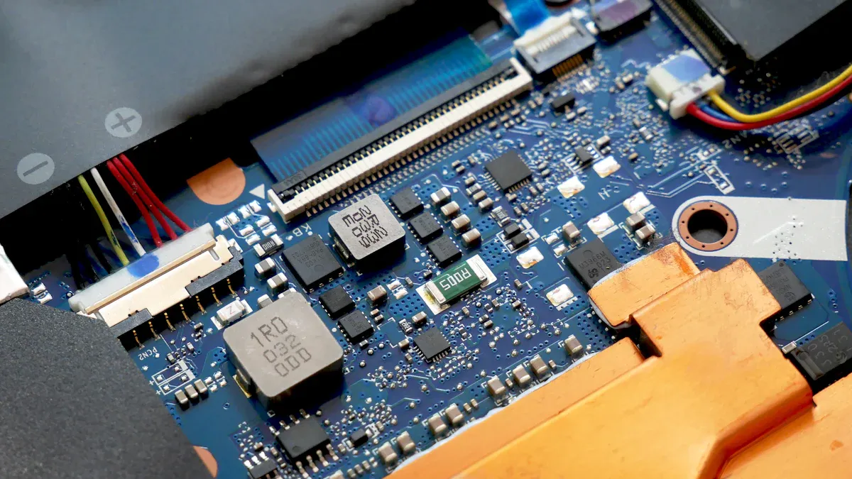
The pcb assembly process creates a populated printed circuit board by mounting components onto a bare pcb. PCB assembly uses advanced automation, robotics, and AI to improve speed and quality. The process includes placing passive and active components, connectors, and fuses onto the board. Unlike pcb manufacturing, which produces the bare printed circuit board, pcb assembly transforms it into a functional pcba. Modern assembly relies on technologies like automated optical inspection and flexible substrates to enhance reliability.
Understanding the assembly steps ensures higher quality and reduces defects in every printed circuit board.
|
Metric |
Value |
|---|---|
|
Market Size (2023) |
|
|
Projected Market Size (2032) |
USD 21.46 Billion |
|
CAGR (2024–2032) |
10% |
-
Common technologies in pcb assembly:
-
Automation and robotics
-
AI-driven design and testing
-
Key Takeaways
-
PCB assembly turns a bare circuit board into a working product by placing and soldering components using advanced machines and skilled workers.
-
Surface Mount Technology (SMT) is the most common method, offering fast production and compact designs, while Through-Hole Technology (THT) provides strong connections for heavy parts.
-
The assembly process includes careful design, solder paste application, precise component placement, soldering, cleaning, and thorough inspection to ensure quality.
-
Choosing the right components and working with certified, experienced assembly partners improves reliability and reduces defects.
-
Common challenges like soldering defects and placement errors can be prevented with good equipment maintenance, design practices, and strong communication with partners.
PCB Assembly vs. Manufacturing
What Is PCB Assembly
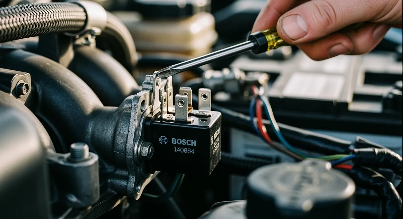
PCB assembly is the process of placing and soldering electronic components onto a printed circuit board. This step turns a bare pcb into a working printed circuit board assembly, or pcba. The assembly process uses machines and skilled workers to mount parts like resistors, capacitors, and chips. Surface mount technology and through-hole technology are common methods. After placement, the assembly goes through soldering, cleaning, and testing. These steps make sure the finished pcba works as designed. Printed circuit board assembly focuses on adding function and reliability to the board.
What Is PCB Manufacturing
PCB manufacturing creates the bare printed circuit board before any components are added. This process uses materials such as FR-4, PTFE, and copper. The steps include drilling holes, etching copper traces, applying solder masks, and printing labels. Manufacturers use Gerber files to guide the design and layout. The finished product is a flat board with copper paths but no electronic parts. Quality control includes electrical tests, automated optical inspection, and X-ray scans. PCB manufacturing builds the foundation for later assembly.
Key Differences
PCB manufacturing and pcb assembly serve different roles in electronics production. Manufacturing builds the physical board, while assembly adds the parts that make it work. The table below shows the main differences:
|
Aspect |
PCB Manufacturing (Fabrication) |
PCB Assembly |
|---|---|---|
|
Creation of bare printed circuit board: etching, drilling, plating, solder mask, silkscreen, testing |
Mounting and soldering electronic components to create a functional circuit |
|
|
Design, etching, drilling, plating, solder mask, silkscreen, finishing, electrical testing |
Component sourcing, solder paste printing, pick and place, soldering, inspection, testing |
|
|
Quality Control |
Visual inspection, AOI, X-ray, electrical testing, stress testing |
Inspection for placement, solder joint integrity, functional testing |
|
Industry Standards |
IPC-A-600 (fabrication quality) |
IPC-A-610 (assembly quality) |
|
Design Files Used |
Gerber files |
Bill of Materials (BOM), pick-and-place files |
|
Outcome |
Physical board with copper paths and protective layers |
Fully populated and functional printed circuit board |
PCB assembly adds complexity, cost, and time due to component selection and testing. Manufacturing focuses on materials and board structure. Both steps are vital for reliable printed circuit board products.
PCB Assembly Technologies
Modern pcb assembly uses several main technologies to meet the needs of electronics production. The most common types of pcb assembly are Surface Mount Technology (SMT), Through-Hole Technology (THT), and Hybrid Assembly. Each method supports different requirements for pcb, production speed, and reliability.
Surface Mount Technology (SMT)
SMT changed pcb assembly in the 1980s. This method places tiny components directly onto the surface of the pcb. SMT allows mounting on both sides of the board, which increases circuit density and reduces size. Most electronics today use SMT because it supports high-volume production and cost efficiency. SMT also speeds up production and lowers labor costs by using automated pick-and-place machines.
|
Advantages of SMT |
Limitations of SMT |
|---|---|
|
Harder to repair due to small parts |
|
|
High component density |
Needs advanced inspection tools |
|
Compact, lightweight devices |
Not ideal for high-power parts |
|
Automatic alignment reduces defects |
Expensive equipment for setup |
SMT accounts for 55% of pcb assembly in 2024 and is expected to grow to 57% by 2025.
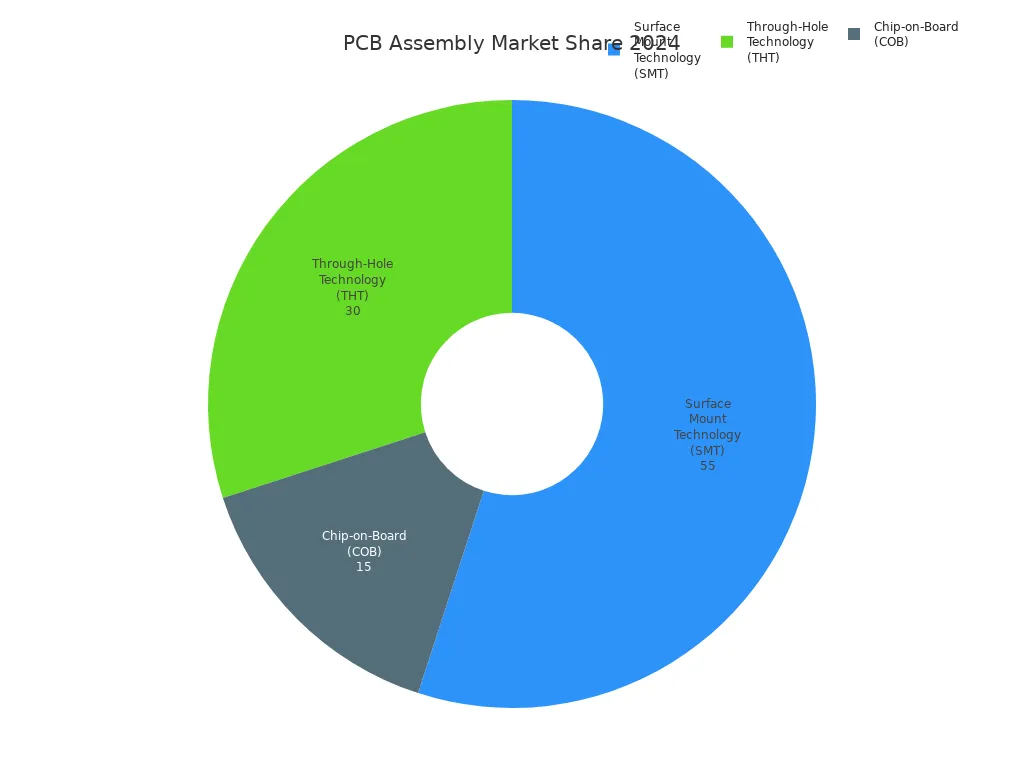
Through-Hole Technology (THT)
THT is an older pcb assembly method. It involves inserting component leads through holes in the pcb and soldering them on the other side. THT provides strong mechanical connections, making it useful for parts that face stress, such as connectors and transformers. THT is common in military, aerospace, and industrial products that need durability. Production with THT is slower than SMT, but it allows easier manual adjustments and repairs.
-
It is preferred for prototyping and testing.
-
THT handles heat and vibration better than SMT.
Hybrid Assembly
Hybrid assembly combines SMT and THT on the same pcb. Production starts with SMT components, then adds THT parts using special soldering methods. This approach gives designers flexibility to use the best technology for each part of the pcba. Hybrid assembly supports complex systems that need both high performance and strong mechanical support. It balances cost, reliability, and production needs for advanced pcb designs.
PCB Assembly Process
Design and DFA
The pcb assembly process begins with careful design and Design for Assembly (DFA). Engineers plan the layout to make the assembly efficient and reliable. They group similar components together and keep their orientation consistent. This helps machines and workers place parts quickly and correctly. Designers use clear polarity markings and silkscreen labels to avoid mistakes. They choose the right footprint sizes and keep enough space between pads for automated placement and inspection.
Some best practices in DFA include:
-
Grouping similar components to optimize pick-and-place operations.
-
Keeping component orientation consistent, especially for polarized parts.
-
Using correct pad sizes and clearances for smt and through-hole parts.
-
Avoiding mixing smt and through-hole components on the same side of the pcb.
-
Adding fiducial marks for machine vision alignment.
-
Providing clear assembly instructions and collaborating with manufacturing teams.
Engineers also consider thermal management by grouping heat-generating parts and planning for heat dissipation. They use panelization to increase production throughput and reduce costs. By following these steps, the design stage sets the foundation for a smooth circuit board assembly process.
Solder Paste Application
Solder paste application is a key step in the pcb assembly process. In high-volume production, manufacturers use a stencil to apply solder paste only where needed. The stencil acts as a template, and a squeegee pushes the paste through the openings onto the pcb pads. The amount of solder paste depends on the stencil thickness and aperture size. Machines control the squeegee pressure, angle, and speed to ensure even coverage.
The most common solder paste types include lead-free, no-clean, water-soluble, and rosin-based pastes. Each type has unique properties:
|
Solder Paste Type |
Key Properties |
Advantages |
Challenges |
Best Use Cases |
|---|---|---|---|---|
|
Lead-Free |
RoHS compliant, melting point ~217-220°C |
Environmentally friendly, strong joints |
Higher melting temp, tin whiskers |
Consumer electronics, aerospace |
|
No-Clean |
Minimal residue, often SAC305 alloy |
No cleaning needed, fast production |
Residue may affect coatings |
IoT, high-volume production |
|
Water-Soluble |
Easily cleaned with water |
Excellent wetting, reliable |
Needs cleaning, residue corrosive |
Medical, aerospace |
|
Rosin |
Mildly active, good shelf life |
Versatile, easy to use |
Sticky residue |
Prototyping, small batches |
Proper solder paste application ensures strong solder joints and reduces defects in the printed circuit board assembly.
Component Placement
After solder paste application, the next step is component placement. Automated pick-and-place machines handle most of this work in high-volume production. These machines use advanced vision systems to place smt components with accuracy as tight as ±0.01 mm. Proper calibration and regular checks keep placement errors low. Even a small misplacement of 0.05 mm can cause soldering defects or electrical problems.
Operators load reels or trays of components into the machines. The machines pick each part and place it on the correct pad. For some complex or large components, skilled workers may place them by hand. Automated optical inspection (AOI) systems check the placement accuracy, looking for errors within ±0.05 mm and ±1 degree rotation.
Accurate placement is critical for the reliability and performance of the pcba. It also helps reduce rework and scrap during production.
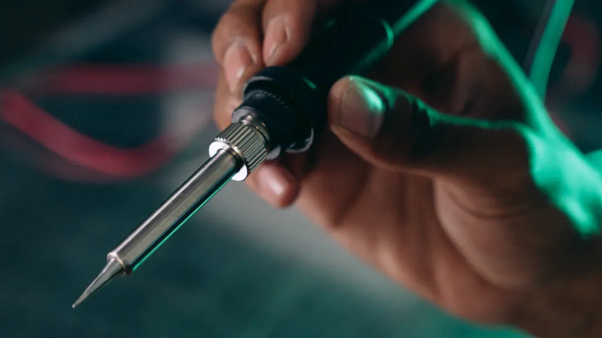
Soldering Methods
Soldering joins the components to the pcb. The most common method in the pcb assembly process is reflow soldering. In this method, the board passes through a controlled oven that melts the solder paste and forms strong joints. Reflow ovens use precise temperature profiles to avoid damaging sensitive components.
For through-hole components, wave soldering is often used. The board moves over a wave of molten solder, which connects the leads to the pads. Both reflow and wave soldering use automated systems to improve consistency and quality.
Proper soldering techniques prevent defects like cold joints, solder bridges, and insufficient solder. High-quality solder materials and correct temperatures are essential. Automated soldering systems help maintain joint consistency and reduce defects, which increases the reliability of the finished pcba.
Cleaning Steps
Cleaning removes flux residues and contaminants left after soldering. Even no-clean flux can leave residues that cause test failures or affect electrical contact. Cleaning is especially important for high-frequency circuits, medical devices, and aerospace applications.
Recommended cleaning steps include:
-
Remove flux residues to prevent corrosion and electrical leakage.
-
Choose the cleaning method based on the flux type:
-
Use solvent-based cleaning (like isopropyl alcohol) for rosin and no-clean fluxes.
-
Use water-based cleaning for water-soluble fluxes.
-
-
Use soft brushes, compressed air, or vacuuming to remove dust and residues.
-
Inspect the pcb after cleaning to ensure no sticky or discolored residues remain.
Following industry standards, such as IPC guidelines, helps ensure the reliability and longevity of the circuit board assembly process.
Inspection and Testing
Inspection and testing are the final steps in the pcb assembly process. These steps verify the quality and functionality of the assembled pcb. Manufacturers use a mix of manual and automated methods to catch defects early.
|
Inspection/Testing Method |
Description |
Typical Application/Notes |
|---|---|---|
|
Inspectors check for placement errors, solder quality, and contamination |
Used for low-volume or complex boards |
|
|
Automated Optical Inspection (AOI) |
Cameras detect surface defects and misplacement |
Fast and accurate for high-volume production |
|
X-ray Inspection (AXI) |
Examines hidden solder joints and internal structures |
Essential for BGAs and multilayer boards |
|
In-Circuit Testing (ICT) |
Electrical probes verify component presence and function |
High-speed verification in mass production |
|
Functional Testing (FCT) |
Simulates real operating conditions |
Ensures the board works as designed |
|
Flying Probe Testing |
Movable probes test connections without fixtures |
Good for prototypes and small batches |
|
Contamination Testing |
Detects harmful residues |
Important for high-reliability products |
|
TDR Testing |
Measures impedance and signal integrity |
Critical for high-speed circuits |
These inspection and testing methods help ensure that every printed circuit board assembly meets quality standards before leaving the production line. Reliable inspection reduces returns and failures in the field, making it a vital part of the pcb assembly process.
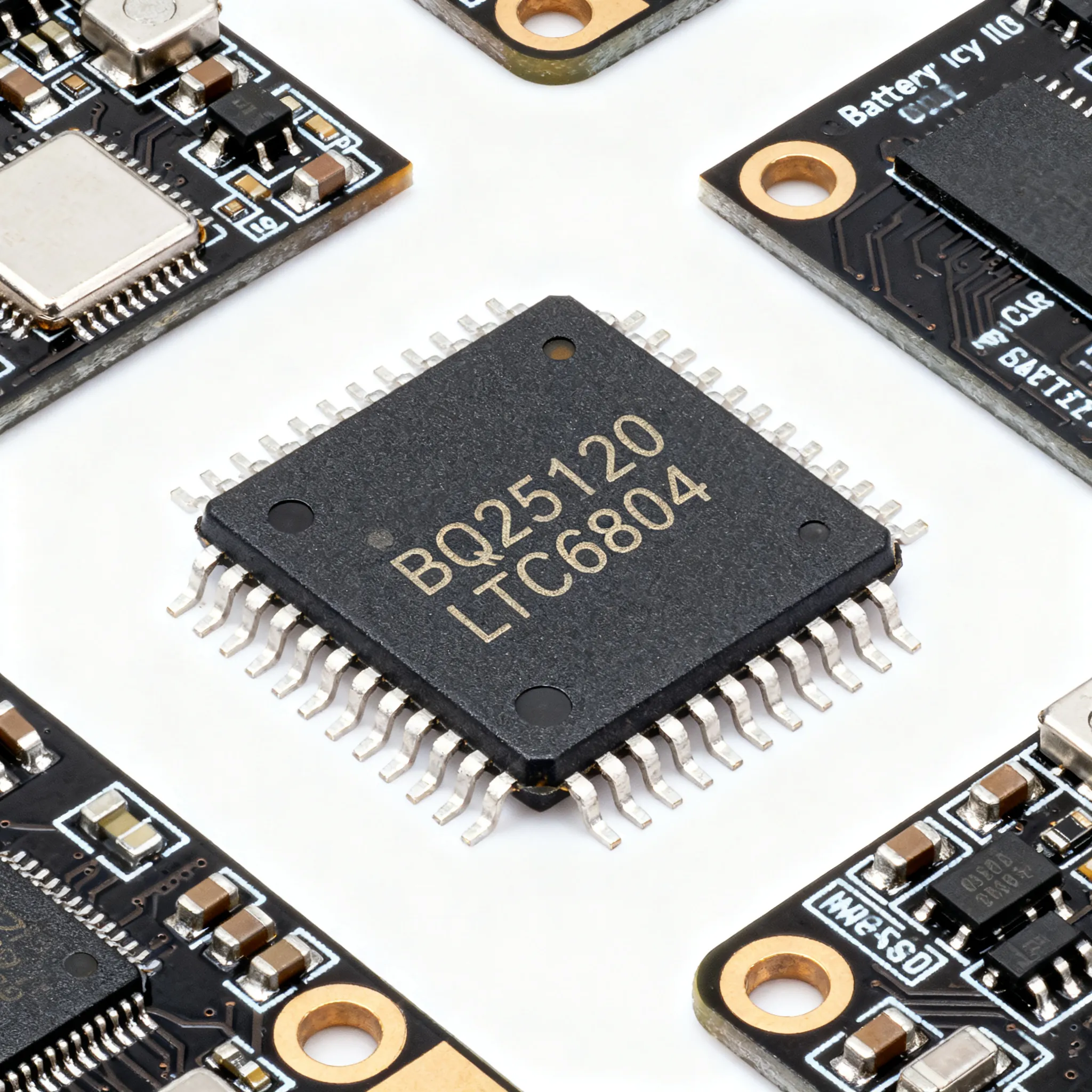
PCB Components
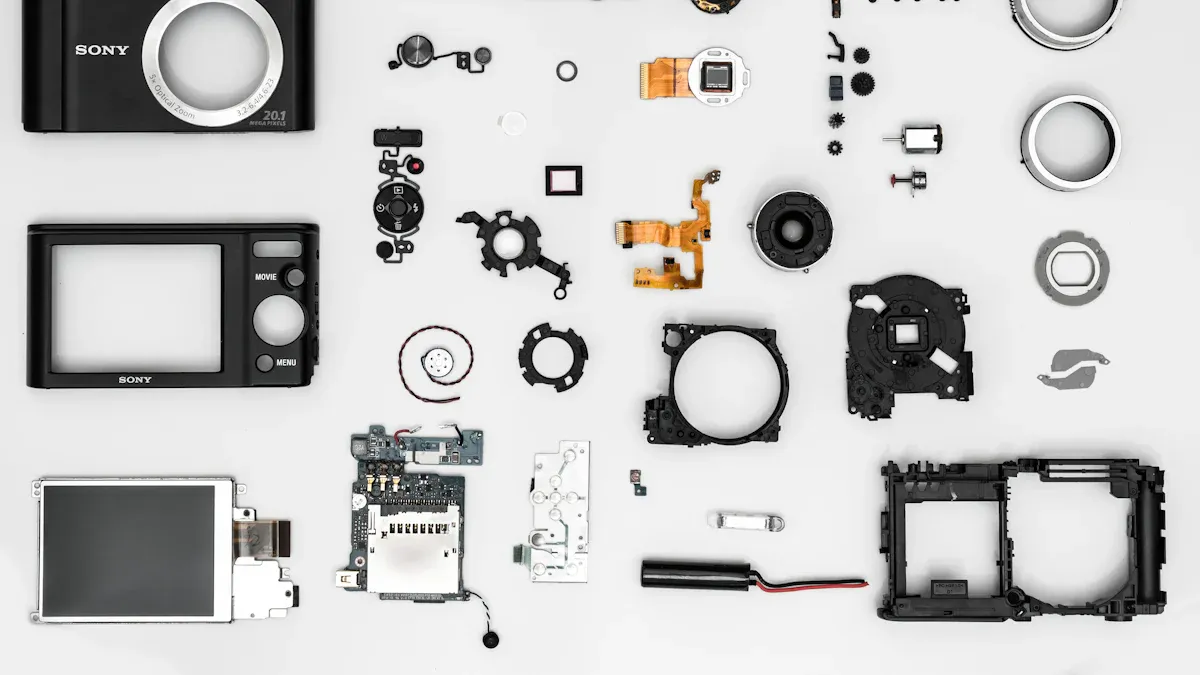
Passive Components
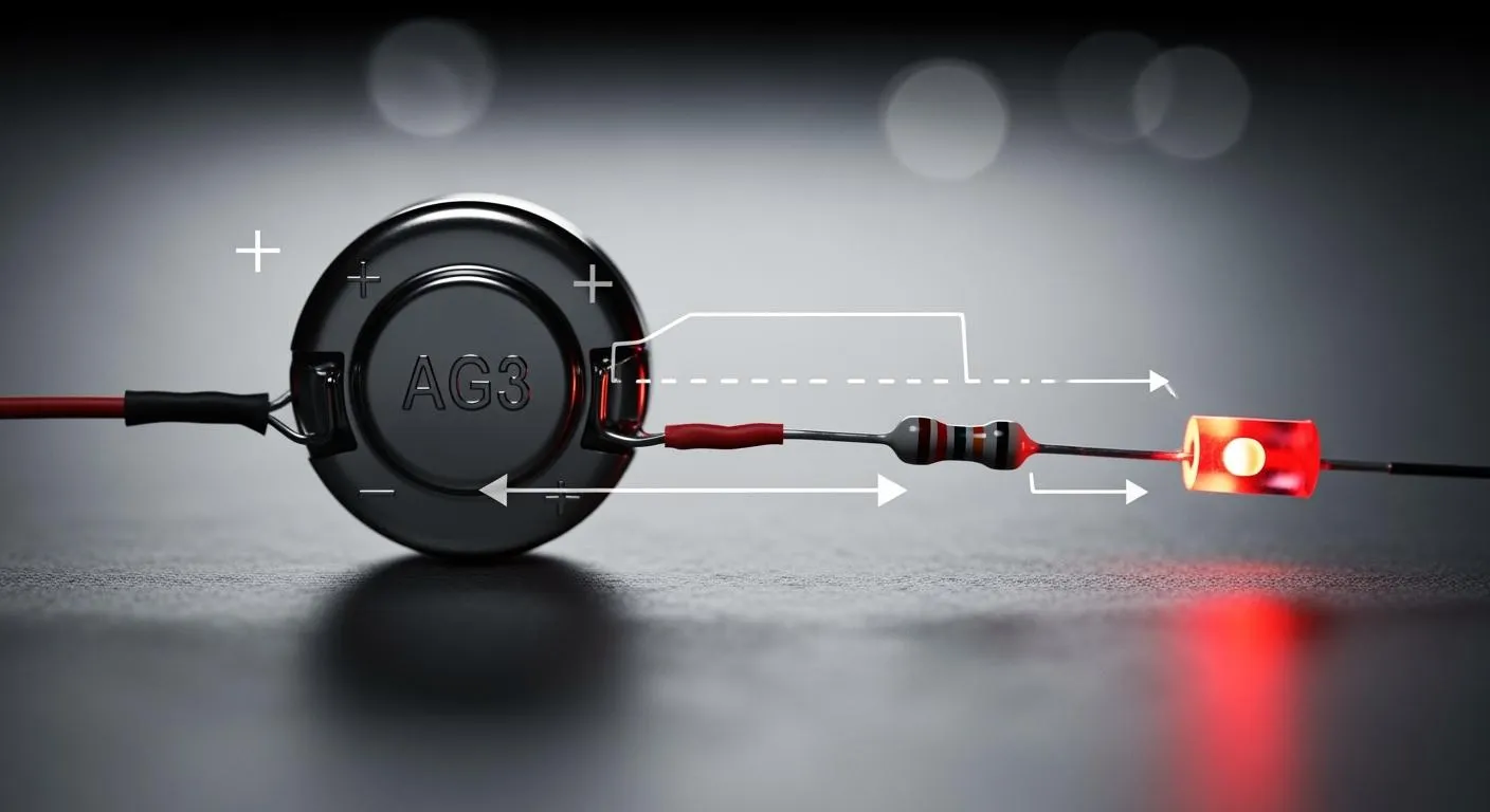
Passive components do not require an external power source to operate. They include resistors, capacitors, and inductors. These parts control current, store energy, and filter signals on a pcb. Resistors limit the flow of current. Capacitors store and release electrical energy. Inductors block changes in current. Designers use these electronic components to manage voltage, reduce noise, and stabilize circuits. Passive components help maintain the reliability and performance of every pcb.
Active Components
Active components need an external power source. They can amplify, switch, or process electrical signals. These parts play a key role in modern pcb designs. The table below shows the main types and their functions:
|
Active Component |
Function Description |
|---|---|
|
Transistors |
Amplify weak electrical signals; act as switches to turn devices on/off; used in power supplies and digital circuits. |
|
Diodes |
Allow current flow in one direction only; used for AC to DC conversion, circuit protection from reverse polarity. |
|
Integrated Circuits (ICs) |
Perform data processing, signal conversion, memory storage; central to modern electronics enabling complex computations and control. |
Active components allow a pcb to perform complex tasks. They enable switching, amplification, and data processing, which sets them apart from passive parts.
Connectors and Fuses
Connectors and fuses protect and link different parts of a pcb. Connectors join boards, cables, or devices, allowing signals and power to flow. Fuses protect circuits from overcurrent and short circuits. Engineers select connectors and fuses based on several criteria:
-
Define application needs, such as load and system criticality.
-
Check voltage and current ratings to match system requirements.
-
Choose the right interrupting rating for safe disconnection.
-
Select fast-acting or time-delay fuses based on response needs.
-
Assess environmental factors like temperature and vibration.
-
Confirm mounting and space requirements.
-
Ensure compliance with standards such as UL 248 or IEC 60127.
-
Pick the best fuse type for the application, such as chip or brick fuses.
-
Review datasheets for size, rating, and certifications.
-
Test under worst-case conditions for reliable protection.
Fuses must meet strict standards to ensure safety and reliability, especially in critical fields like automotive and medical devices.
Selection Tips
Choosing the right electronic components for pcb assembly ensures quality and compatibility. Engineers check physical compatibility, such as footprint and pin alignment, to avoid assembly issues. They confirm electrical compatibility by matching pinouts and considering signal integrity. Power supply must meet voltage and current needs. Designers account for tolerance and temperature effects, especially in precision circuits. Good thermal management, such as using heat sinks, helps maintain performance.
Other important tips include:
-
Select components with stable supply and long lifecycles to avoid redesigns.
-
Balance cost and performance for an optimized bill of materials.
-
Use parts from reputable manufacturers to reduce field failures.
-
Prefer components that fit standard assembly processes to lower defect rates.
-
Ensure compliance with RoHS and other environmental standards.
Collaboration with pcb assembly partners helps improve manufacturability and reliability. Careful selection of components leads to better performance and longer-lasting pcb products.
Common Challenges
Many manufacturers face common challenges in pcb assembly that can affect the quality and reliability of the final product. These issues often appear during production and can lead to costly rework or failures in the field.
Soldering Defects
Soldering defects remain one of the most frequent problems in pcb assembly. These defects can weaken connections or cause short circuits. Some typical soldering issues include:
-
Gaps in solder joints from not enough solder paste or misaligned components.
-
Solder balling caused by impurities or too much heat.
-
Cold solder joints when the solder does not heat properly.
-
Solder bridging, which creates unwanted connections between pads.
-
Component shift due to movement during soldering.
-
Lifted pads from excessive heat or vibration.
-
Webbing and splashes from poor solder paste or cleaning.
-
Sunken joints and tombstoning, often linked to thermal imbalance.
-
Shadowing, where components do not fully contact the solder.
Proper control of solder paste, temperature, and equipment maintenance helps reduce these defects during production.
Placement Issues
Accurate placement of components on the pcb is critical for reliable assembly. Placement issues can arise from several sources:
-
Equipment problems, such as pick-and-place machine calibration errors or worn nozzles.
-
Material issues, including bent leads, warped boards, or inconsistent pad sizes.
-
Process errors, like incorrect placement parameters or programming mistakes.
-
Environmental factors, such as temperature changes or dust in the production area.
-
Design errors, including centroid file mistakes or unclear assembly drawings.
To prevent these problems, manufacturers perform regular equipment maintenance, control material quality, optimize placement processes, and verify design files before production.
PCB Damage
PCB damage can occur at many stages of production. The most common types include:
-
Heat-related issues, such as warped boards or delamination, often result from poor thermal management.
-
Contamination from flux residues, fingerprints, or dust can cause electrical failures.
-
Documentation errors, like outdated instructions, may lead to assembly mistakes.
-
Equipment calibration problems can create defects if machines are not properly maintained.
-
Physical damage, such as scratches or broken traces, often happens during handling.
Manufacturers use clean rooms, digital documentation, regular training, and advanced inspection methods like AOI and X-ray to prevent and detect damage. Good design practices, such as proper component spacing and thermal relief, also help reduce risks.
Tip: Addressing these common challenges in pcb assembly early in the production process leads to higher yields and more reliable products.
Quality and Partner Selection
Certifications
Certifications show that a company meets industry standards for quality and safety. Many customers look for these certifications before choosing a provider. The table below lists the most recognized certifications in the PCB assembly industry:
|
Certification |
Description |
Importance in PCB Assembly |
|---|---|---|
|
IPC (IPC-A-610) |
Sets standards for assembly quality and inspection. |
Ensures consistent assembly quality. |
|
ISO 9001:2015 |
Quality management system standard. |
Improves process control and customer satisfaction. |
|
RoHS |
Limits hazardous substances in electronics. |
Promotes safe and eco-friendly manufacturing. |
|
UL Listing |
Safety standard for fire and electrical risks. |
Required for products used in harsh or regulated environments. |
|
ITAR |
Controls defense-related manufacturing. |
Needed for military and defense projects. |
|
MIL (MIL-STD) |
Military standards for performance and reliability. |
Used in high-reliability and military applications. |
A company with these certifications can deliver reliable pcb assembly services and meet strict industry requirements.
Capabilities
A strong PCB assembly partner offers a wide range of technical skills. Companies should check if the partner uses Surface Mount Technology (SMT), Through-Hole Assembly, and mixed technology. They should also look for experience with fine pitch and Ball Grid Array (BGA) assembly. Handling multi-layer boards is important for complex projects. Design for Manufacturability (DFM) analysis helps improve designs before production. In-house testing, such as Functional Testing (FCT), In-Circuit Testing (ICT), Automated Optical Inspection (AOI), and X-ray inspection, ensures product quality. Reliable partners also support prototyping, quick-turn production, and have strong supplier relationships. Fast turnaround and the ability to scale from prototype to mass production help meet changing project needs.
Collaboration Tips
Good communication leads to better project outcomes. Companies should set up clear lines of contact and share accurate project files, such as BOMs and Gerber files. Regular updates help everyone stay on track. Quick responses to questions prevent delays. Teams should work together to solve problems and improve processes. Early design reviews with all parties can catch issues before production. Using standard file formats and collaborative tools makes teamwork easier. Sharing feedback and lessons learned helps everyone improve for future projects.
Tip: Strong collaboration and clear communication with your assembly partner reduce mistakes and speed up delivery.
PCB assembly brings together advanced technologies, careful design, and precise processes to create reliable electronics. Each step, from design to inspection, plays a vital role in quality. Industry reports highlight several keys to success:
-
Select experienced partners with a strong track record.
-
Check for high-quality standards and certifications.
-
Assess manufacturing capabilities for complex designs.
-
Verify thorough inspection and testing methods.
-
Prioritize fast lead times and transparent pricing.
-
Value strong customer support and communication.
Choosing the right partner and following best practices help ensure dependable results. Readers can explore industry standards or case studies for deeper knowledge.
FAQ
What is the difference between SMT and THT in PCB assembly?
Surface Mount Technology (SMT) places components directly on the board’s surface. Through-Hole Technology (THT) inserts component leads through holes in the board. SMT supports smaller, faster devices. THT provides stronger connections for heavy or high-stress parts.
How do manufacturers check for defects in PCB assembly?
Manufacturers use Automated Optical Inspection (AOI), X-ray machines, and manual checks. AOI finds placement errors. X-ray reveals hidden solder joints. Manual inspection catches visible problems. These steps help ensure each board meets quality standards.
Why is cleaning important after soldering?
Cleaning removes flux and dirt left from soldering. Residue can cause corrosion or short circuits. Clean boards last longer and work better. High-reliability products, like medical devices, always require careful cleaning.
What should engineers consider when choosing PCB components?
Engineers should check size, voltage, and compatibility. They review datasheets and select parts from trusted brands. Good choices help prevent failures and make assembly easier.