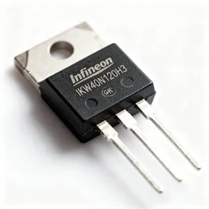
Never Confuse IGBT Versus MOSFET Again With This Guide
An engineer's choice between an Insulated Gate Bipolar Transistor (IGBT) and a Metal-Oxide-Semiconductor Field-Effect Transi
An engineer's choice between an Insulated Gate Bipolar Transistor (IGBT) and a Metal-Oxide-Semiconductor Field-Effect Transistor (MOSFET) is critical for modern power electronics. The market for these components reflects this importance. It is projected to grow significantly, underscoring the need for engineers to master this technology. This guide clarifies the igbt versus mosfet decision. It helps engineers select the right transistor for new designs or find a suitable replacement MOSFET.
The fundamental difference is straightforward. A Metal-Oxide-Semiconductor Field-Effect Transistor is a fast, voltage-driven transistor ideal for switching applications. An IGBT, a different type of transistor, is a powerful, high-voltage transistor built for demanding power applications. Understanding this core distinction is the first step in mastering power electronics technology.
Key Takeaways
- MOSFETs switch fast and work well for high-frequency tasks. IGBTs handle high power and high voltage.
- When replacing a MOSFET, check its on-resistance (Rds(on)), gate charge (Qg), safe operating area (SOA), and thermal resistance. These ensure good performance.
- MOSFETs are best for applications above 50kHz. IGBTs are best for high-power tasks below 50kHz.
- New technologies like SiC MOSFETs and advanced IGBTs are changing how we choose between them. The best choice depends on the specific job.
Key Parameters for a Replacement MOSFET
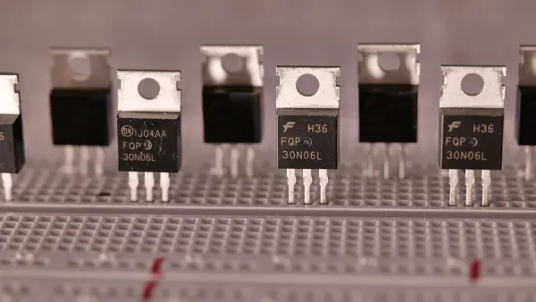
Selecting a replacement MOSFET requires a careful review of its datasheet. An engineer must match or improve upon the original component's key characteristics to ensure reliability and performance. Four parameters are especially critical in this process. A failure to properly evaluate these characteristics can lead to poor efficiency, overheating, or catastrophic failure of the mosfet circuit.
Rds(on): On-Resistance and Efficiency
The on-resistance, or Rds(on), is the electrical resistance between the drain and source terminals when the MOSFET is fully turned on. This value directly governs the component's conduction losses and overall efficiency.
Replacement Rule: Choose a MOSFET with an equal or lower Rds(on).
A lower Rds(on) value means the MOSFET presents less resistance to current flow. This reduction minimizes power loss, which is dissipated as heat. The power (PD) a MOSFET consumes follows the formula PD = Rds(on) x ID².
For example, a MOSFET with a 50mΩ Rds(on) carrying a 10A current generates 5W of heat. A replacement MOSFET with a 20mΩ Rds(on) generates only 2W under the same load. This significant reduction in heat improves energy efficiency and simplifies thermal management.
Choosing a MOSFET with a higher Rds(on) than the original part introduces serious risks:
- Reduced Efficiency: The new MOSFET will generate more heat, wasting power and lowering system efficiency.
- Current Unbalance: In circuits with parallel MOSFET devices, the MOSFET with a higher Rds(on) will carry less current. This forces other devices to handle more load, causing uneven heat distribution and potential failure.
- Thermal Issues: Increased heat generation from a higher Rds(on) can push the MOSFET beyond its thermal limits, especially if the existing thermal management system is not designed for the extra load. Rds(on) also increases with temperature, creating a dangerous cycle where more heat leads to higher resistance and even more heat.
Qg: Gate Charge and Switching Speed
Total Gate Charge, or Qg, is the amount of electrical charge required to turn the MOSFET on completely. It is a key indicator of the mosfet performance in switching applications. A lower gate charge allows the MOSFET to transition between its on and off states more quickly.
Replacement Rule: Choose a MOSFET with an equal or lower Qg, especially for high-frequency applications.
The relationship between gate current (Ig), gate charge (Qg), and switching time (tsw) is Ig = Qg / tsw. This shows that switching speed is directly limited by how fast the gate charge can be supplied or removed.
- A smaller Qg value leads to faster switching speeds and lower switching losses.
- In high-frequency designs, a low gate charge is critical for maintaining high efficiency. Reducing Qg from 80nC to 20nC in a 100kHz switching circuit can cut switching losses by 75%.
- The Gate-to-Drain Charge (Qgd), or "Miller charge," is a component of Qg. It is particularly important because it determines the duration of the Miller Plateau, a period where both high voltage and high current exist across the MOSFET, directly causing switching power losses.
A replacement MOSFET with a significantly higher Qg will switch slower. This increases switching losses, generates more heat, and reduces the overall efficiency of the power conversion stage.
SOA: The Safe Operating Area Map
The Safe Operating Area (SOA) is one of the most important graphs in a MOSFET datasheet. The SOA chart defines the voltage and current limits within which the MOSFET can operate without damage or degradation. It is a critical map for ensuring long-term reliability.
Replacement Rule: The SOA of the replacement MOSFET must completely encompass all operating points of the original part.
An SOA graph plots the drain-to-source voltage (Vds) against the drain current (Id). The bounded area shows the conditions the MOSFET can safely handle. Operating outside this area risks immediate destruction.
Understanding the SOA Boundaries The SOA is limited by several factors:
- Rds(on) Limit: At low Vds, the maximum current is limited by the MOSFET's on-resistance.
- Power Dissipation Limit: The device's ability to dissipate heat limits operation.
- Secondary Breakdown Limit: At high Vds, localized current flows can cause thermal runaway and destroy the MOSFET. The SOA graph includes a limit to prevent this.
- Maximum Voltage/Current Limit: The absolute maximum ratings for Vds and Id form the outer boundaries of the SOA.
Choosing a wide SOA MOSFET is crucial for robust designs. A MOSFET can survive brief VGS spikes if the resulting power dissipation remains within its thermal and SOA limits. However, sustained operation outside the guaranteed safe operating area will lead to failure. For complex designs where operating points push the limits of the SOA, consulting with experts is wise. For instance, a HiSilicon-designated solutions partner like Nova Technology Company (HK) Limited) can provide guidance on selecting a robust wide SOA MOSFET for demanding applications. A wide SOA MOSFET provides a larger margin of safety against unexpected power surges or load changes. Selecting a wide SOA MOSFET ensures better performance and reliability. Therefore, a wide SOA MOSFET is a superior choice. Always use a wide SOA MOSFET for critical applications.
Thermal Resistance and Heat Dissipation
Thermal resistance, noted as RθJC (junction-to-case), measures how effectively heat travels from the MOSFET's internal silicon junction to its outer case. It is measured in degrees Celsius per watt (°C/W). This parameter is fundamental to the thermal performance of the MOSFET.
Replacement Rule: Choose a MOSFET with an equal or lower thermal resistance.
A lower thermal resistance value indicates better heat transfer, allowing the MOSFET to run cooler for a given power loss. This is essential for reliability, as high temperatures degrade a MOSFET over time. Excellent thermal management starts with selecting a component with good thermal characteristics.
The junction temperature (Tj) can be estimated with a simplified equation:
Tj = Tamb + Pd * (RθJC + RθCS + RθSA)
Here, Tamb is the ambient temperature, Pd is the power dissipated, and the Rθ terms are the thermal resistances of the junction-to-case, case-to-heatsink, and heatsink-to-ambient, respectively.
A replacement MOSFET with poor thermal performance (high thermal resistance) will run hotter. This leads to severe consequences:
- Reduced Lifespan: High temperatures accelerate failure mechanisms like silicon damage and packaging degradation.
- Decreased Efficiency: As the MOSFET heats up, its Rds(on) increases, which in turn increases conduction losses and generates even more heat.
- Thermal Runaway: In worst-case scenarios, the device's temperature can rise uncontrollably until it fails catastrophically. This poor thermal performance can compromise the entire system.
While these four mosfet characteristics are the most critical for a replacement, a complete selection process involves a matrix of factors. Engineers should also review other datasheet parameters, including threshold voltage (Vth) and device capacitances, to ensure full compatibility and stable performance.
IGBT Versus MOSFET: The 2025 Showdown
The choice between an IGBT and a MOSFET defines the performance of modern power electronics. Historically, the decision was simple. A MOSFET was for high-speed switching, and an IGBT was for high-power loads. Today, advancements in mosfet technology and transistor integration are blurring these lines. This creates a competitive landscape where the best transistor for an application is not always obvious. The igbt versus mosfet debate now centers on a dynamic crossover zone.
The MOSFET Zone: High Frequency
A MOSFET excels in high-frequency applications. Its primary advantage is its incredible switching speed. This high-speed capability allows engineers to design smaller, more compact systems because it reduces the required size of passive components like inductors and capacitors. The dominance of the MOSFET is clear in any application operating above 50kHz.
The superior efficiency of a MOSFET at high frequencies comes from its fundamental structure. A MOSFET is a majority-carrier device. This means it does not suffer from the "tail current" that slows down an IGBT's turn-off process. This absence of tail current dramatically reduces switching losses.
- Faster Switching: A Silicon Carbide (SiC) MOSFET turns on and off much faster than an IGBT, minimizing energy loss during each switching cycle.
- Lower Losses: The inherent properties of SiC mosfet technology lead to a substantial reduction in overall switching losses. For example, replacing an IGBT with a SiC MOSFET in a 2kVA inverter can reduce power loss per transistor by approximately 41%.
This high-speed performance makes the MOSFET the ideal transistor for the following applications:
| Switching Frequency | MOSFET Applications |
|---|---|
| 80kHz and above | Switching power supplies (DC-DC converters), phone chargers, and other low-power, high-frequency devices. |
The IGBT Zone: High Power
The IGBT is the undisputed champion in high-power, high-voltage applications. Its unique structure combines the simple gate drive of a MOSFET with the high-current and low-saturation-voltage capability of a bipolar transistor. This hybrid design makes it a robust and efficient transistor for demanding loads.
An IGBT's ability to handle immense power stems from a process called conductivity modulation. During conduction, the IGBT injects minority carriers (holes) into its drift region. This process drastically reduces the transistor's internal resistance. This allows the IGBT to manage much higher current densities than a MOSFET of the same size, especially at blocking voltages above 400V. This structural advantage gives the IGBT superior performance in high-power circuits.
The primary benefit is a lower on-state voltage drop. This directly reduces conduction losses, which is a critical factor for high-efficiency in high-power systems. The bipolar nature of the IGBT transistor enhances its current-carrying ability, minimizing heat generation and improving overall system efficiency.
This makes the IGBT the go-to transistor for many industrial and consumer applications:
- Motor drives (air conditioners, industrial motors)
- Uninterruptible Power Supplies (UPS)
- Induction heating (cooktops, microwave ovens)
- Renewable energy inverters
The Crossover Battleground
The most interesting part of the igbt versus mosfet showdown happens in the "crossover battleground." This zone typically covers applications in the 400V to 1000V range with switching frequencies between 10kHz and 50kHz. In this area, both the MOSFET and the IGBT are viable options, and the best choice depends on a careful analysis of total power losses.
An engineer must calculate the total losses to make the right decision. This is the sum of conduction losses and switching losses.
Total Loss (P_total) = Conduction Loss (P_cond) + Switching Loss (P_sw)
- Conduction Loss is the power lost when the transistor is on. It is higher in a MOSFET at high currents.
- Switching Loss is the power lost during the on/off transitions. It is higher in an IGBT due to its slower switching speed.
The igbt versus mosfet decision depends on which loss component dominates in a specific application.
2025 Trends: The Game is Changing
The future of power electronics is being shaped by rapid innovation in both mosfet and IGBT technology.
Rise of the Advanced MOSFET: New generations of Silicon Carbide (SiC) MOSFET devices are pushing aggressively into traditional IGBT territory. This advanced mosfet technology offers compelling performance benefits. Gen 4 SiC MOSFETs provide higher efficiency, faster switching, and better thermal management. Their ability to operate at higher temperatures and voltages in a smaller package makes this transistor an attractive alternative for electric vehicles and high-power industrial drives, promising high-performance designs.
Evolution of the Intelligent IGBT: Simultaneously, the IGBT is not standing still. The latest IGBT Intelligent Power Modules (IPMs) represent a massive leap in integration and efficiency. These modules combine an IGBT with optimized gate drivers and protection circuits into a single package. The integration of wide-bandgap materials like SiC into these modules is projected to reduce power losses by up to 50% in high-voltage systems. This technology delivers a high-efficiency solution with robust protection, making this transistor ideal for next-generation renewable energy systems and smart factory automation.
Ultimately, the choice in the crossover zone is becoming more complex. The high-speed performance of a modern SiC MOSFET challenges the IGBT's dominance, while the smart integration of an IGBT IPM offers a powerful, reliable, and high-performance solution. A deep understanding of the application's specific power and switching requirements is essential for navigating this evolving landscape.
Engineers can master the igbt versus mosfet choice with a clear checklist. This simplifies decisions in modern power electronics.
Decision Checklist 📝
- MOSFET: Choose this mosfet for high-frequency (>50kHz) and low-voltage (<400V) applications. A mosfet is ideal for DC-DC converters.
- IGBT: Select this transistor for high-power (>600V) and lower-frequency (<50kHz) systems. It excels in motor drives.
When replacing a mosfet, an engineer must select a new mosfet that matches or improves upon the original mosfet's Rds(on), Qg, SOA, and thermal resistance. A superior mosfet ensures reliability.
The future of power electronics is dynamic. Advanced SiC mosfet technology and efficient IGBT IPM technology are blurring traditional boundaries. This evolution in power electronics makes the choice for a mosfet or IGBT more nuanced than ever. The right mosfet depends on a deep analysis of application needs.
FAQ
What is the most critical factor for a replacement mosfet?
🗺️ The Safe Operating Area (SOA) is paramount. The replacement mosfet must have an SOA that fully covers the original part's operating points. A robust SOA ensures reliability. A wide SOA provides a safety margin. The SOA is a critical map for safe operation, so a wide SOA is best.
Why is fast switching important for a mosfet?
⚡ Fast switching reduces power loss. A mosfet with quick switching transitions minimizes the time high voltage and current exist together. This improves system efficiency. Faster switching also allows for smaller components, leading to more compact designs. Excellent switching performance is key for high efficiency.
Can a mosfet have a good SOA but poor efficiency?
Yes. A mosfet can have a wide SOA but high on-resistance (Rds(on)). The wide SOA indicates it can handle voltage and current spikes safely. However, high Rds(on) increases conduction losses, which lowers overall efficiency. The SOA does not guarantee efficiency.
How does switching speed affect total losses?
Switching speed directly impacts switching losses. Slower switching increases the energy lost during each on/off cycle. For high-frequency applications, these switching losses can dominate. Optimizing switching speed is crucial for achieving high efficiency. A fast switching mosfet is essential for high-frequency efficiency.