How to Read and Interpret Integrated Circuit Diagrams for PCB Design
When you start reading circuit boards, you must know integrated circuit diagrams and their schematic symbols. Each schematic is like a map. It shows you how to connect parts. It also helps you follow signals.
When you start reading circuit boards, you must know integrated circuit diagrams and their schematic symbols. Each schematic is like a map. It shows you how to connect parts. It also helps you follow signals. If you know standard symbols, pinouts, and connections, you can avoid mistakes. This helps you make good designs. Today, many companies use AI to help read schematics better.
|
Aspect |
Description |
Correlation with Schematic Interpretation Accuracy |
|---|---|---|
|
AI Adoption Rise |
AI models help find more mistakes and read schematics better |
|
|
Performance Gains |
AI finds more mistakes with better accuracy |
Better finding helps you trust the schematic reading |
You can learn these basics if you practice. This guide will help you. Soon, you can read integrated circuit diagrams with confidence.
Key Takeaways
-
Learn the usual schematic symbols and reference names. This helps you read circuit diagrams well and avoid errors.
-
Always check pinouts, netlists, and signal flow two times. This makes sure your PCB connections match the schematic and work right.
-
Place parts on your PCB with care. Keep power parts cool and line up parts to make assembly easy and help them work better.
-
Use careful routing like wide traces for power and short paths. This helps lower noise and stops signal problems.
-
Check your schematic and PCB layout very well to find mistakes early. Talk clearly with your PCB maker for the best results.
Integrated Circuit Diagrams
Basics
When you start a PCB project, you look at integrated circuit diagrams. These diagrams show how to connect the parts. Most schematics use rectangles with pins. Each pin has a number and a label. The schematic works like a map. It helps you place and connect each part on your board. You use the schematic to plan where each part goes. It also shows how signals move between parts.
If you know the basics of schematics, you get better PCB results. For example, one electronics company found that designers who understood schematics made boards with fewer mistakes. Their boards had better signal integrity. Look at the table below. It shows how good schematic knowledge helps improve important areas:
|
Parameter |
Standard Design |
Advanced Design |
|---|---|---|
|
-15 |
-3 |
|
|
Thermal Performance (°C) |
85 |
70 |
|
Power Integrity (mV ripple) |
50 |
20 |
|
EMI Reduction |
N/A |
Significant |
You can see that learning schematic basics helps you make better choices.
Symbols
You will see many symbols in every schematic. Each symbol stands for a different part. Standard symbols make it easy to read any schematic. These symbols follow rules from groups like IEEE and ANSI.
-
Groups like IEEE and ANSI set the rules for circuit symbols in the United States.
-
IEEE Std 315 (ANSI Y32.2) is an old but important standard for these symbols.
-
IEEE Std 91 gives the rules for logic gate symbols.
-
There are also international standards like IEC. These have small differences but work the same way.
When you learn these symbols, you can read schematics from any company or country.
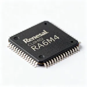
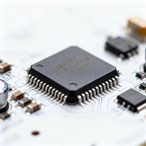
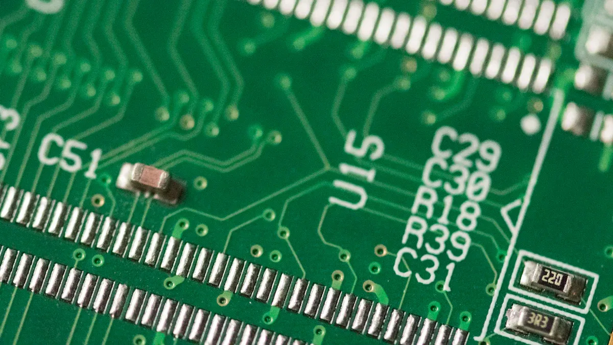
Reference Designators
Every schematic uses reference designators. These are short codes like U1, R2, or C3. Each code points to a certain part. You use these codes to match parts in the schematic to parts on your PCB. Unique codes help you avoid mistakes. If you do not use unique codes, you might mix up parts or make errors.
If reference designators are missing or blocked, you can have problems during testing and making the board. Clear and correct codes help keep your schematic and PCB matched. This reduces mistakes and makes your board easier to test.
Schematic Connections
Understanding schematic connections helps you build a better circuit board. You need to know how to read pinouts, netlists, and signal flow. Each part of the schematic gives you clues about how the printed circuit board will work. When you learn these skills, you can design a circuit board that works well and is easy to test.
Pinouts
Pinouts show you how each pin on an integrated circuit connects to the rest of the circuit board. You will see numbers and labels next to each pin in the schematic. These numbers match the pins on the real part. You must check the schematic to see which pin does what job. Some pins give power, some send signals, and others connect to ground.
Tip: Always double-check the pinout in the schematic before you place the part on your printed circuit board. Mistakes here can cause the circuit board to fail.
You can use a table to keep track of pin functions:
|
Pin Number |
Label |
Function |
|---|---|---|
|
1 |
VCC |
Power Supply |
|
2 |
IN |
Signal Input |
|
3 |
OUT |
Signal Output |
|
4 |
GND |
Ground |
When you match the schematic pinout to the real part, you make sure your circuit board works as planned. If you mix up the pins, the printed circuit board may not work at all.
Netlists
A netlist is a list of all the connections in your schematic. It tells you which pins connect together. You use the netlist to make sure every part of your circuit board connects the right way. The netlist acts like a checklist for your printed circuit board.
You can find the netlist in your schematic software. It looks like this:
Net1: U1-1, R1-2, C1-1
Net2: U1-2, R2-1
Net3: U1-3, C2-2, GND
Each line shows which pins connect together. You follow the netlist to lay out the traces on your printed circuit board. If you miss a connection in the netlist, your circuit board will not work right.
Note: Always compare the netlist to the schematic before you start making the printed circuit board. This step helps you catch mistakes early.
Signal Flow
Signal flow shows you how electricity moves through the schematic and the circuit board. You start at the input and follow the path to the output. You look for closed loops, which means the current can travel from the source, through the parts, and back to ground.
You can use arrows in the schematic to trace the signal flow. This helps you see how the circuit board will work. If you find a break in the signal path, you know the printed circuit board will not work.
-
Start at the input pin in the schematic.
-
Follow the lines to each part.
-
Check that every signal has a path to ground or to the next part.
-
Make sure there are no open ends.
If you follow the signal flow in the schematic, you can spot problems before you build the circuit board. This step saves you time and money.
Alert: If you do not trace the signal flow, you might miss a broken connection. This can make your printed circuit board useless.
When you understand pinouts, netlists, and signal flow in the schematic, you can design a circuit board that works the first time. You will also find it easier to fix problems if they come up.
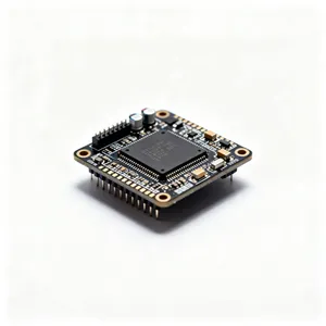
Printed Circuit Board Layout
Placement
When you move from a schematic to a printed circuit board, you start with component placement. You want to arrange each part so the circuit board works well and is easy to build. Place heavy connectors as through-hole parts for strong support. Use surface-mount parts for smaller, lighter components, but keep them away from tight corners to avoid routing problems.
-
Keep all parts facing the same way. This helps you avoid mistakes during assembly.
-
Place power parts near the edge of the circuit board or close to vents. This keeps them cool.
-
Leave space around sensitive chips like BGAs. You need at least 1-2mm for repairs.
-
Do not put heavy parts near the edge. This can cause the circuit board to crack.
Tip: Use thermal simulation tools to find hot spots on your printed circuit board. Move parts if you see too much heat in one area.
Routing
After you place the parts, you connect them with traces. Good routing keeps your circuit board reliable. Use a solid ground plane under high-speed signals. This helps your printed circuit board avoid noise and keeps signals clean. Place vias in a grid to spread out current. Use 135° bends in traces instead of sharp corners. This reduces signal problems.
|
Parameter |
Impact on Circuit Board |
Recommendation |
|---|---|---|
|
Handles more current |
Use wide traces for power |
|
|
Trace Spacing |
Stops crosstalk |
Space traces by signal speed |
|
Trace Layout |
Manages heat |
Short, direct paths |
Keep traces short and direct. This helps your circuit board work better and last longer.
Translating Schematic
You turn a schematic into a printed circuit board by following clear steps:
-
Start with a complete schematic. Make sure all parts and connections are correct.
-
Check the schematic with simulation tools to catch errors.
-
Set up your printed circuit board layers for signals, power, and ground.
-
Place each part on the circuit board using the schematic as your guide.
-
Route the traces, following the schematic connections.
-
Run checks for signal quality and errors.
-
Create files for making and assembling the circuit board.
Note: Always match the schematic to the printed circuit board layout. This keeps your circuit board free from mistakes.
Common Mistakes
Errors
When you read and interpret integrated circuit diagrams, you can make mistakes that affect your PCB design. Many designers face the same problems. You can avoid these errors if you know what to look for.
-
You might define system boundaries in a way that is too broad or unclear. This can cause overlapping failure events and make your analysis confusing.
-
Sometimes, you may go into too much detail when analyzing the circuit. This can waste time and does not always help your design.
-
If you do not have all the data or if the data is wrong, you can misunderstand how parts of the circuit affect each other.
-
You may not fully understand the system or its parts. If you skip using extra tools like Failure Mode and Effects Analysis (FMEA), you can miss important errors.
-
If you do not use detailed schematics, block diagrams, or process flow diagrams, you can misinterpret how the circuit works.
Tip: Always gather all the documents and diagrams before you start your design. This helps you see the whole picture and avoid missing details.
Solutions
You can fix most common mistakes by following a few simple steps. A study of hundreds of schematics found that missing power sources caused 21% of critical errors, and 18% of errors came from connecting multiple outputs to one net. Even small mistakes, like mismatched voltage levels, can stop your PCB from working.
-
Check that holes are not too close to copper traces. This keeps your board strong and safe.
-
Make sure the annular rings around holes are big enough. This helps with soldering and stops breakage.
-
Compare your Gerber files with your schematic. This prevents wrong part placement and routing errors.
-
Talk clearly with your PCB maker. Good communication stops misunderstandings and delays.
-
Watch out for stubs in traces, wrong trace widths, and space issues. These can cause signal problems or power loss.
-
If you are new to PCB design, ask for help or use design checks to catch mistakes early.
🛠️ Careful review and teamwork help you avoid costly errors and build a reliable PCB.
Practice Example
IC Diagram Walkthrough
You can learn a lot by looking at a simple schematic. Imagine you have a basic amplifier circuit. The schematic shows a rectangle for the chip, lines for wires, and symbols for resistors and capacitors. Each pin on the chip has a number and a label. You see how the input signal goes into one pin, passes through a resistor, and then connects to the output pin. The ground and power pins connect to the rest of the circuit board.
A good schematic acts like a map. It helps you see how each part connects. You can follow the lines to trace the signal path from start to finish.
When you read integrated circuit diagrams, always check that every pin matches the real chip. Use the schematic as your guide. This step helps you avoid mistakes when you build your circuit board.
PCB Design Example
Now you can turn your schematic into a real printed circuit board. Start by placing each part on your design software. Put the chip in the center. Place the resistors and capacitors close to the pins they connect to. Draw traces to match the lines in your schematic. Make sure every connection in the schematic appears on your circuit board.
The MorePCB resource explains that your schematic is the blueprint for your circuit board. The layout must match the logic of the schematic. If you skip this, your circuit board may not work. Always cross-check your schematic and your layout. This step keeps your design safe from errors.
A tutorial from Physics Forums shows a simple example. The schematic and the PCB layout look almost the same. The tracks on the board connect the same parts as the lines in the schematic. This process proves that you can translate a schematic into a working circuit board if you follow each step.
Remember: Careful checking at each stage helps you build a reliable circuit board.
You have learned the main steps for reading circuit boards. You also know how to turn schematics into working PCBs. If you follow a step-by-step process, you make fewer mistakes. This helps you get better results.
-
Always use clear schematics and pinouts.
-
Carefully copy each connection to your layout.
-
Try each tutorial to get better at these skills.
Using step-by-step methods, like the Kepner-Tregoe process, helps you find and fix problems for good. Automated inspection tools make your work more accurate. Keep learning and look for more resources to become great at PCB design.
FAQ
What is the most important thing to check in a schematic before starting PCB design?
You should always check that every connection in the schematic matches the real parts. Make sure all pin numbers and labels are correct. This step helps you avoid mistakes when you build your circuit board.
How do you know which symbol stands for each part?
Look for the standard symbols in your schematic. Each symbol has a unique shape. For example, a rectangle often means an integrated circuit. You can use a symbol chart or legend if you feel unsure.
Tip: Keep a printed symbol chart near your workspace for quick reference.
Why do you need reference designators like U1 or R2?
Reference designators help you match each part in the schematic to the real part on your board. They make it easy to find and place parts during assembly and testing. Without them, you might mix up parts or miss connections.
What should you do if you find a missing connection in your netlist?
If you see a missing connection, go back to your schematic and check the wiring. Fix any open ends or mistakes. Then update your netlist. This step keeps your circuit board working as planned.
🛠️ Careful checking saves you time and prevents errors.