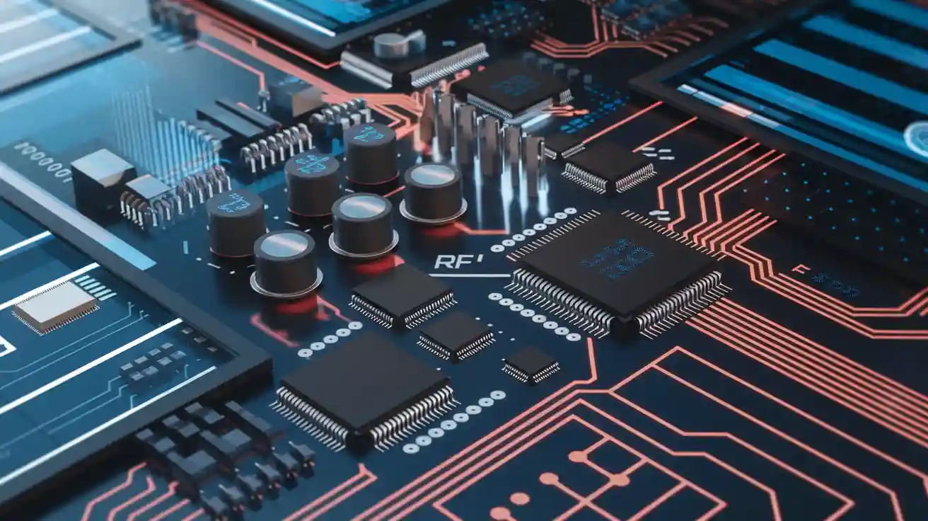
Essential RF Components for Modern PCB Designs
Modern rf pcb designs use many important rf components. These parts help the board work fast and keep signals strong and steady. Antennas send and receive electromagnetic signals.
Modern rf pcb designs use many important rf components. These parts help the board work fast and keep signals strong and steady. Antennas send and receive electromagnetic signals. This is important for how far the system can reach. Filters pick certain frequency bands and block signals you do not want. Amplifiers make weak signals stronger so they are easier to use. Impedance matching circuits are very important in antenna feed lines, low-noise amplifiers, and power dividers. These rf components are the main parts of any fast rf pcb. Careful pcb layout makes sure each part works well. Engineers work hard on good pcb layout to stop problems and make the rf pcb work better.
Tip: Good pcb layout and putting rf components in the right place help stop signal loss and make the board work better.
Key Takeaways
-
Pick the right RF parts like amplifiers, filters, and antennas. This helps signals stay strong and clear in your PCB design.
-
Use PCB materials with low dielectric constant and loss. These help signals move faster and lower signal loss at high frequencies.
-
Make your PCB layout with care. Match impedance, keep traces short, and put parts close together. This helps lower noise and signal loss.
-
Use solid ground planes and shielding. These block interference and keep your RF signals clean and steady.
-
Use simulation and design software to test your RF PCB first. This saves time and helps you avoid expensive mistakes.
RF Components Overview
Active Components
Active rf components are very important in rf pcb designs. These parts need power from outside to work. They change, boost, and switch signals on rf circuit boards. The main active parts are amplifiers, low-noise amplifiers (LNAs), mixers, and oscillators.
|
Component |
Primary Function |
Key Characteristics |
|---|---|---|
|
Signal amplification |
Gain, noise figure, output power, bandwidth |
|
|
Mixers |
Frequency conversion |
Conversion gain, noise figure, isolation |
|
Oscillators |
Signal generation |
Frequency stability, phase noise, output power |
Amplifiers make weak signals stronger so the rf circuit board can use them. LNAs help make the signal-to-noise ratio better at the start of the receiver path. Mixers change signal frequencies. This helps with sending and getting signals in wireless systems. Oscillators make steady signals that work as timing or carrier waves. These active rf components are needed for sending and getting signals in high-frequency rf uses.
Passive Components
Passive rf components do not need power to work. They are resistors, capacitors, and inductors. These parts shape signals and help other rf components work better.
Resistors control current, set bias points, and help manage noise in rf circuit design. Capacitors store energy and block DC but let AC signals go through. They also filter noise and help tune circuits. Inductors store energy in magnetic fields and block high-frequency signals. This is important for filtering and tuning. In high-frequency circuits, engineers must pick passive parts with low parasitic values and tight tolerances. This keeps signals strong and lowers losses on the rf pcb.
Note: When picking passive rf components, engineers should check frequency response, impedance matching, and parasitic elements like ESR and ESL. Small package sizes, like 0402, help lower unwanted inductance and make rf circuit boards work better.
Filters and Resonators
Filters and resonators pick the right frequencies and block bad signals. They keep rf circuit boards free from noise and interference. Filters use resistors, capacitors, and inductors to let only some frequencies pass. Resonators, like cavity or ceramic types, help keep signals steady and lower electromagnetic interference.
|
Filter/Resonator Type |
Description/Characteristics |
Typical Applications |
|---|---|---|
|
Use acoustic wave resonance in piezoelectric layers; good power handling and temperature stability |
5G wireless communications |
|
|
Ceramic Filters |
High-permittivity ceramic materials for compact resonators |
Consumer electronics, communication devices |
|
Crystal Filters |
Quartz crystal resonance for narrow bandwidth and high selectivity |
High frequency stability applications, precise filtering |
|
Microstrip Filters |
Planar PCB filters; compact, easy integration, good microwave performance |
Microwave frequency filtering, space-constrained applications |
|
Waveguide Filters |
Hollow metal structures guiding EM waves; high power and frequency performance |
High frequency, high power RF systems |
Filters and resonators are used in wireless systems, radar, and navigation devices. They help rf circuit design by keeping signals clean and steady. This is very important for high-frequency rf work.
Attenuators and Circulators
Attenuators and circulators control signal levels and flow on rf circuit boards. Attenuators are passive parts that make signals weaker. They help stop distortion and make impedance matching better. Engineers use them to control gain and avoid noise problems in rf pcb layouts.
Circulators are special ferrite devices that send signals in one direction. They stop unwanted reflections and lower interference. This keeps signals moving well and protects sensitive rf parts. Circulators are important in complex rf circuit board layouts where signal quality matters.
Power Splitters and Combiners
Power splitters and combiners share signals across rf pcb designs. Wilkinson dividers are a common type. They split one input signal into two or more outputs with equal power and phase. This keeps signals balanced and lowers losses.
-
Wilkinson splitters have low insertion loss and good isolation between outputs.
-
They keep phase the same, which is important for phased array antennas and communication systems.
-
Important things to check are insertion loss, isolation, phase balance, and power handling.
When adding splitters and combiners to an rf circuit board, engineers must pick materials with stable dielectric properties. This makes sure signals are shared evenly and lowers losses, especially in high-frequency rf uses.
Antennas
Antennas send and get electromagnetic waves. They connect rf circuit boards to the outside world. The antenna you pick changes signal range, direction, and how well the system works.
|
Antenna Type |
Description |
Advantages |
Typical Applications |
|---|---|---|---|
|
Zigzag shape for longer antenna in small area |
Covers broad frequency range; low cost; easy PCB printing |
IoT, RFID systems |
|
|
Dipole |
Two conductive elements in a straight line |
Simple manufacturing; bidirectional emission; decent gain (~2.15 dBi) |
TV broadcasting, Wi-Fi |
|
Patch |
Flat rectangular patch with ground plane |
Thin, lightweight; high gain; customizable polarization; directional |
GPS, satellite communications |
|
Loop |
Circular or rectangular conductive loop |
Small size; omnidirectional; covers various frequencies |
RFID, NFC, wireless devices |
|
Slot |
Slot cut in PCB ground plane |
Saves space; good bandwidth and radiation; customizable design |
Radar, Wi-Fi devices |
Antenna choice depends on frequency, board size, cost, and direction needs. Good antenna placement and matching networks help make signals strong and lower interference. In rf pcb design, engineers must keep antennas away from noisy parts and follow layout rules to get the best results.
RF PCB Materials
High-Frequency Laminates
Engineers pick special pcb substrate material for rf pcb designs that need to work fast. High-frequency laminates keep electrical properties steady and lower signal loss. These materials help signals stay strong in fast circuits. The table below lists some popular high-frequency laminates, their dielectric properties, and where they are used.
|
Material |
Manufacturer |
Dielectric Constant (Dk) Range |
Dissipation Factor (Df) Range |
Key Features and Applications |
|---|---|---|---|---|
|
Rogers RO4000 Series |
Rogers Corporation |
3.38 – 6.15 |
0.002 – 0.003 |
Excellent electrical performance; compatible with FR4 processing; ideal for mid-frequency RF designs |
|
RT/duroid® Series |
Rogers Corporation |
Varies by grade |
Very low |
High-end laminate with extremely low loss; used in aerospace, military, and high-frequency microwave applications |
|
PTFE / Teflon |
Various suppliers |
2.1 – 2.5 |
Extremely low |
Superior signal performance with ultra-low loss; processing is challenging and costly |
|
Taconic Laminates |
Taconic |
2.2 – 10 |
0.0009 – 0.0037 |
Highly customizable, low-loss materials suitable for a wide range of RF/microwave needs |
|
F4B / F4BM Series |
Chinese brands (e.g., Bicheng PCB) |
2.2 – 4.5 |
0.001 – 0.005 |
Affordable alternative for less demanding high-frequency applications; good performance for the price |
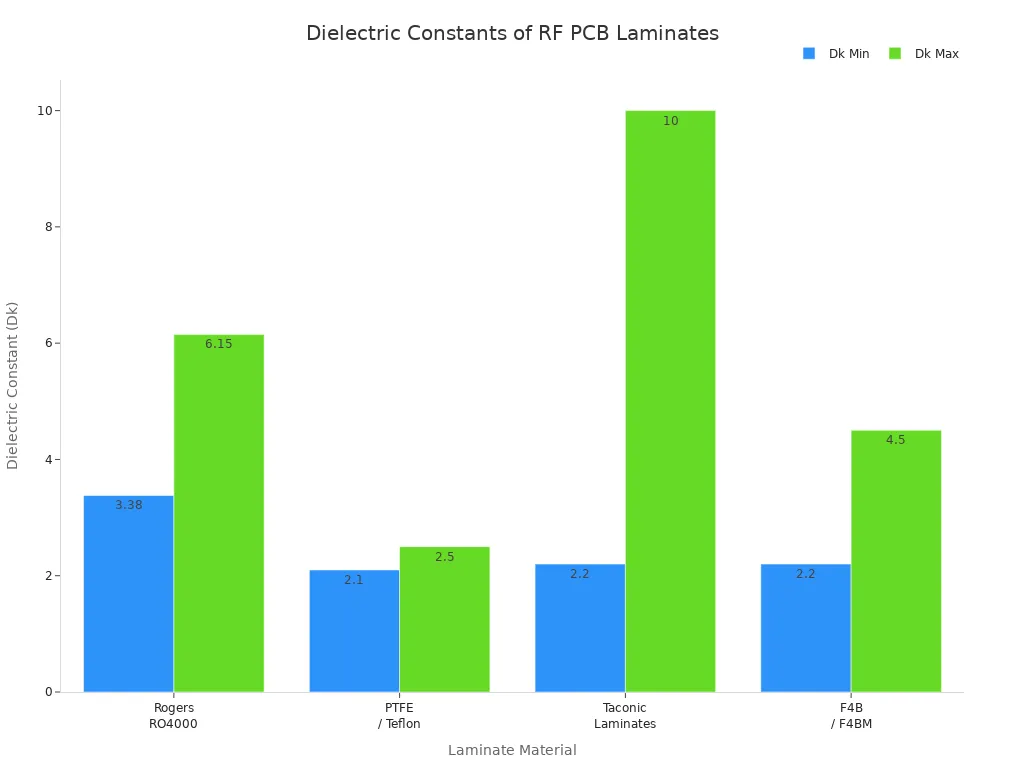
PTFE-based laminates, like those from Rogers, have very low loss tangent and can handle heat well. These features make them great for fast and high-frequency rf pcb designs. FR4, a common pcb substrate material, does not work well above 2.5 GHz because it has a higher dielectric constant and loss tangent.
Material Selection Tips
Picking the right pcb substrate material is very important for fast rf pcb performance. Engineers want materials with low dielectric constant and low dissipation factor. These features help signals move faster and lower signal loss. Here are some things to think about:
-
Dielectric constant (Dk) should be under 4 for better signal speed.
-
Dissipation factor (Df) should be less than 0.005 to lower signal loss.
-
Insertion loss comes from conductor loss, dielectric loss, radiation loss, and leakage loss.
-
Coefficient of thermal expansion (CTE) must match in mixed stack-ups to stop warping.
-
High thermal conductivity helps get rid of heat.
-
Dielectric thickness changes impedance and signal strength.
-
Material anisotropy and the environment can change electrical properties.
-
Manufacturing compatibility makes sure the pcb substrate material works with drilling, lamination, and plating.
Material choice also affects how easy it is to make the board and the cost. PTFE and other fast materials work very well but are harder to make and cost more. Using more than one material can help balance cost and performance in high-frequency pcb design.
Impact on Signal Integrity
The dielectric constant of a pcb substrate material changes how fast signals move through the rf pcb. For example, FR4 has a dielectric constant of about 4, which makes signals slower than PTFE or ceramic materials. Fast signals need steady dielectric properties to stop reflections and signal loss. High-frequency laminates keep their dielectric constant steady even when temperature or frequency changes, which helps keep signals strong.
Loss tangent is also important. FR4 has a loss tangent around 0.020, but high-frequency laminates have values near 0.004. Lower loss tangent means less signal loss at high frequencies. Fast designs do better with materials that do not soak up much water and can handle heat. Controlled impedance routing, based on the pcb substrate material, is needed to stop reflections and keep signals strong in fast rf pcb designs.
RF PCB Design Essentials
Impedance Matching
Impedance matching is very important in rf pcb design. Engineers match the impedance of rf traces to the source and load. This helps stop signal reflection and power loss. Good impedance matching keeps signals strong and clear. This is needed for fast rf pcb circuits.
Some common impedance matching methods are:
-
Lumped element matching uses separate inductors and capacitors. L-networks are good for simple changes. Pi-networks give more options and can also filter signals.
-
Transmission line matching uses quarter-wave transformers and stub matching. These work best at higher frequencies.
-
The Smith Chart lets engineers see complex impedance. It helps them pick the right matching parts.
-
Simulation software, like Advanced Design System (ADS), CST Studio Suite, and Ansys HFSS, helps engineers check impedance matching before making the rf pcb.
Engineers often use microstrip and stripline transmission lines to control impedance. Keeping a steady 50-ohm impedance is standard in rf pcb design. This helps lower reflections and makes power transfer better. Engineers also use termination resistors for high-speed digital signals. These help match impedance and lower reflections.
Tip: Always check Voltage Standing Wave Ratio (VSWR) and Return Loss. Low VSWR and high Return Loss mean better impedance matching and less signal reflection.
Transmission Lines
Transmission lines move rf signals across the rf pcb. The most common types are microstrip, stripline, and coplanar waveguide. Each type changes signal quality in different ways.
|
Feature/Aspect |
Stripline Transmission Line |
|
|---|---|---|
|
Location on PCB |
Signal trace on external PCB layer |
Signal trace embedded between two ground planes inside PCB |
|
Dielectric Environment |
Mixed dielectric (substrate + air) |
Uniform dielectric (substrate only) |
|
EMI Susceptibility |
More susceptible to EMI |
Strong EMI shielding |
|
Radiation Loss |
Present, especially at high frequencies |
Negligible radiation loss |
|
Impedance Stability |
Variable impedance |
More stable and consistent impedance control |
|
Manufacturing Complexity |
Simpler and cost-effective fabrication |
More complex and expensive fabrication |
|
Typical Applications |
General RF, wireless devices |
High-speed digital, aerospace, EMI-sensitive applications |
Microstrip lines are on the surface of the rf pcb. They are easy to make and test. But they can lose more signal at high frequencies. Stripline runs between two ground planes inside the board. This gives better shielding and more stable impedance. Engineers use microstrip for general rf pcb work. They use stripline for fast or noise-sensitive designs.
Coplanar waveguide structures also help control impedance. They can lower crosstalk. Engineers pick the right transmission line based on frequency, noise needs, and cost.
Note: Keep rf traces as short as you can. Shorter traces lower signal loss and reduce unwanted coupling.
Stack-Up and Trace Design
Stack-up and trace design affect how signals move through the rf pcb. Good stack-up choices help control impedance and lower crosstalk. They also make signal integrity better.
Best practices for stack-up and trace design are:
-
Use low-loss dielectric materials with dielectric constants from 2.2 to 3.5. Keep dissipation factors below 0.005 to lower signal loss in fast circuits.
-
Put ground planes right under signal layers. This gives a clear return path and can cut crosstalk by up to 30% at 2.4 GHz.
-
Keep dielectric thickness steady. Even small changes can shift impedance by several ohms.
-
Make stack-ups symmetrical. Symmetry stops board warping and keeps impedance steady.
-
Do not use sharp 90-degree bends in rf traces. Use 45-degree or curved traces to lower signal reflections.
-
Use fewer via transitions. Too many vias can change impedance, especially above 3 GHz.
-
Use simulation tools to check impedance and signal quality before making the board.
-
Keep power and ground planes close together. A small gap increases interplane capacitance and lowers power supply noise.
Callout: Following pcb design rules, like using global ground planes and placing reflection planes, helps keep signals strong and lowers noise.
Engineers should also follow rf layout rules to keep rf traces away from noisy digital circuits. Good rf routing and careful placement of rf interconnects help stop unwanted coupling and signal loss. By following these pcb layout tips, engineers can make reliable rf circuit boards that work well in fast and high-frequency uses.
Grounding and Shielding
Ground Planes
A ground plane is a key part of any RF PCB. Engineers use a solid ground plane to give signals a path back with low resistance. This helps cut down noise and blocks electromagnetic interference by a lot, up to 20 dB. They put many ground vias close to fast parts. These vias make the return path resistance less than 1 ohm. This keeps noise low. Star grounding links different ground spots at one point. This stops noise from moving between board sections. If the board has a strange shape, the ground plane should match it closely. If the ground plane must split, engineers add stitching vias or capacitors where high-frequency signals cross. They also put decoupling capacitors near each power pin. This lowers ground bounce and keeps voltage steady. A good ground plane makes the board more reliable and keeps signals clear.
Shielding Techniques
Shielding keeps RF circuits safe from outside noise. Engineers pick different materials for shielding, and each one has its own good points.
|
Material |
Properties and Benefits |
|---|---|
|
Conducts well, absorbs and redirects electromagnetic waves, easy to solder, bends easily, resists rust. |
|
|
Brass |
Cheap, resists rust and wear, has good electrical resistance, easy to shape. |
|
Aluminum |
Light, strong, conducts well, not expensive, resists rust. |
|
Gold |
Great for high-frequency shielding, used for coating, good for phones and WiFi routers. |
Shielding can be made from sheet metal, metal foam, or mesh screens. Sometimes, the shield has holes or mesh to block certain signals. Engineers pick the best material and shape for the device’s needs. Shielding is very important in medical, military, and banking systems to stop electromagnetic interference.
Isolation Strategies
Isolation keeps RF signals clean by stopping crosstalk and interference. Engineers keep RF traces away from digital or fast signals. They split the ground plane to keep RF areas apart from digital or power parts. Guard rings around sensitive parts and via fences near RF traces help with isolation. Shielding at the board or part level also keeps RF signals inside. These steps stop unwanted coupling and help the board work well. Good isolation helps the board meet electromagnetic rules and keeps signals clear in high-frequency designs.
Thermal and Power Management
Heat Dissipation
High-power RF PCB parts can get very hot when working. Getting rid of heat is important to keep these parts safe and working well. Engineers use different ways to move heat away from hot spots on RF PCBs.
|
Heat Dissipation Method |
Description and Benefits |
|---|---|
|
Thick Copper Traces |
Thick copper traces spread out heat and lower resistance. |
|
Groups of small holes help move heat to ground planes or heat sinks. |
|
|
Small copper pieces under hot parts send heat right to copper planes or heat sinks. |
|
|
Board Material Selection |
Materials like aluminum, copper, or ceramic move heat fast and help cool the board. |
|
PCB Layout Optimization |
Putting hot parts away from sensitive areas and using wide traces stops hot spots and helps air move better. |
Engineers also use heat sinks and special pads to help heat move away. Metal-core PCBs, like ones with aluminum backs, cool better than regular FR-4 boards. Some boards use fans to cool very hot systems. Engineers use computer tools and cameras to find hot spots before making the final board.
Tip: Good heat control helps parts last longer and keeps RF signals steady.
Power Distribution
How power moves on the RF PCB changes how well it works. Engineers follow some simple rules to make sure power is steady:
-
Power and ground planes just for power keep voltage steady and cut noise.
-
Decoupling capacitors near active parts stop voltage spikes and keep signals clean.
-
Wide copper traces and good paths lower resistance and stop overheating.
-
Thermal vias and heat sinks help cool power parts.
-
Good planning and grounding lower noise and keep signals strong.
-
Computer checks before making the board help find power problems early.
Picking the right board material is important too. Boards that move heat well and lose little signal work better. Engineers often keep analog and digital ground planes apart to stop noise. These steps help RF PCBs work well and last a long time, even in tough places.
Component Placement in RF PCB
Placement Best Practices
Engineers use simple pcb layout rules to stop signal loss and noise. They follow these steps to help the rf circuit board work well:
-
Put high-frequency parts close together. This keeps traces short. Short traces help signals stay strong and keep input impedance steady.
-
Group parts that do the same job. This makes routing easier and lowers electromagnetic interference.
-
Make sure all parts face the same way, especially ICs and polarized parts. This helps stop mistakes when putting the board together.
-
Leave enough space between parts and from the board edge. At least 40 mil between parts and 100 mil from the edge helps stop shorts and makes routing easier.
-
Keep digital, analog, RF, and power parts apart. This stops crosstalk and keeps signals clean.
-
Use a solid ground plane under RF parts. This gives a good return path and lowers noise.
Tip: Putting similar parts together also helps heat move away. This keeps the rf circuit board stable.
Minimizing Parasitics
Parasitic effects can make signals worse on any pcb layout. Engineers use these ways to keep unwanted effects low:
-
Do not use sharp 90-degree bends in traces. Smooth curves help keep signals strong.
-
Keep traces short, straight, and smooth. This lowers parasitic inductance and capacitance.
-
Use as few vias as you can on high-frequency traces. Each via adds unwanted inductance and capacitance.
-
Put important signals on the top layer. This helps lower parasitic effects.
-
Keep a clean, solid ground return path under RF traces. Ground vias help keep the ground strong.
-
Keep sensitive RF signals away from digital traces to stop noise.
A solid ground plane and careful part placement help lower noise and keep signals strong. Following pcb design rules keeps parasitic effects low.
Integration with Digital Circuits
Mixing digital and RF parts on the same pcb layout needs careful planning. Engineers keep digital and RF areas apart to stop crosstalk. They use ground planes to shield RF signals from digital noise. Decoupling capacitors near power pins filter out voltage spikes and keep signals clean. Enough space between traces, at least three times the trace width, helps stop crosstalk. Shielding sensitive parts with copper pours or guard traces protects them from outside noise. Following pcb design rules for mixed-signal boards helps keep signals strong and the board reliable.
Tools for RF PCB Design
Design Software
Engineers use special computer programs to make RF PCBs. These programs help them draw circuits and put parts in the right place. The software checks if everything is connected right. Good design software makes work faster and helps stop mistakes. Many programs have lists of RF parts and show the board in 3D. Some popular programs are Altium Designer, Cadence Allegro, and Mentor Graphics Xpedition. These tools let engineers draw circuits, change layouts, and check for errors. They also let teams share files with each other. Using these programs helps engineers find and fix problems before making the board.
Tip: Picking software with RF part lists and simulation tools saves time and helps you get things right.
Simulation and Testing
Simulation and testing tools help engineers check RF PCB designs before making them. These tools show how signals move and act on the board. Engineers use them to find problems like weak signals, crosstalk, and impedance mismatches. Keysight Advanced Design System (ADS) is a top tool for RF and microwave PCB simulation. It checks signal strength, power, and 3D electromagnetic effects. ADS can do special tests, like harmonic balance and nonlinear modeling, which are needed for high-frequency designs.
Engineers also use Ansys SIwave, Cadence Sigrity, and Mentor Graphics HyperLynx. These tools check signal and power strength, electromagnetic noise, and heat problems. Altium Designer with Ansys is a good choice for small teams. The table below lists some of the most used simulation and testing tools:
|
Tool Name |
Key Features |
Use in RF PCB Verification |
|---|---|---|
|
Keysight ADS |
Integrated RF simulation, EM analysis, layout checks |
Accurate RF and microwave PCB verification |
|
Ansys SIwave |
Signal/power integrity, EMI, 3D EM analysis |
Finds impedance mismatches and EMI issues |
|
Cadence Sigrity |
High-speed analysis, parasitic extraction, thermal co-simulation |
Ensures signal and power integrity |
|
Mentor Graphics HyperLynx |
Fast simulation, power integrity, user-friendly interface |
Efficient for complex RF PCB testing |
|
Altium Designer + Ansys |
Unified design and simulation, PDN visualization |
Verifies designs before fabrication |
Before making the board, engineers run these tests to make sure everything works. This step helps stop expensive mistakes and makes sure the RF PCB will work well.
Picking, placing, and putting together RF components the right way makes RF PCBs work well. Engineers make the board better and more reliable by using smart steps:
-
Pick parts that have the right features for the job.
-
Put parts in spots that help stop noise and keep signals strong.
-
Try out designs with computer tools before making the board.
Tip: You can learn more about RF PCB design by checking online classes, reading guides from companies, and joining tech forums.
FAQ
What is the most important RF component for beginners to understand?
Amplifiers are key. They make weak signals stronger. Beginners should learn how amplifiers work and why signal strength matters in RF circuits.
How does PCB material affect RF performance?
PCB material changes how signals move. Materials with low loss and stable dielectric constant keep signals strong. Engineers pick materials like PTFE or Rogers for high-frequency designs.
Why do engineers use ground planes in RF PCBs?
Ground planes give signals a safe path back. They lower noise and block interference. A solid ground plane helps the board work better and keeps signals clear.
Can digital and RF circuits share the same PCB?
Yes, but engineers keep them apart. They use ground planes and shielding to stop noise. Careful layout helps both digital and RF parts work well together.
What tools help test RF PCB designs?
Engineers use simulation software like Keysight ADS and Ansys SIwave. These tools check signal strength, impedance, and noise before making the board.