Essential IC Package Types Every Electronics Engineer Should Know
You should know about Essential IC Package Types because electronics change a lot. IC packages started simple, like DIP, but now there are new types like BGA and flip-chip.
You should know about Essential IC Package Types because electronics change a lot. IC packages started simple, like DIP, but now there are new types like BGA and flip-chip. These changes happen because people want smaller and faster devices. They also want devices to be more powerful. The package you pick changes how your device handles heat. It also affects how reliable it is and how it fits in your design. When you choose a package, you need to think about what your device needs. You also have to think about what is possible to do. Making good choices helps you keep costs low. It also helps your device work well and last longer.
Key Takeaways
-
IC packages change how big, fast, and reliable a device is. They also affect how much heat it makes. Pick the right one for your project.
-
Through-hole packages like DIP are simple to use and fix. They need more space and work best for slow designs.
-
Surface-mount packages save space and make things work better. They help make products faster but need special tools and care.
-
Pin grid array packages like BGA have lots of connections and fast signals. They need good inspection and design skills.
-
Newer packages like CSP and WLP help make devices smaller and lighter. They may need more care for heat and fixing.
Essential IC Package Types Overview
Classification by Mounting
There are three main ways to put IC packages on a circuit board. These are through-hole, surface-mount, and pin grid array packages. Each one connects to the board in its own way. Each type also has special features.
|
Package Type |
Mounting Method |
Description & Examples |
|---|---|---|
|
Through-Hole |
Pins inserted through PCB holes |
This group has Dual Inline Package (DIP) and Single Inline Package (SIP). The pins go through the board and get soldered underneath. |
|
Surface-Mount |
Leads soldered on PCB surface |
This group has Small Outline Package (SOP), Quad Flat Package (QFP), and Ball Grid Array (BGA). The leads sit on top of the board pads. |
|
Pin Grid Array (PGA) |
Can be through-hole or socketed |
The pins are in a grid shape. These are often used for microprocessors. You can plug them into sockets or put them on the board surface. |
Most new designs use surface-mount packages. They take up less space and cost less money. They also make building things faster. Through-hole packages are still good for strong connections and testing ideas. They are also used for high-power parts. Pin grid arrays are easy to swap out and are used in CPUs a lot.
Key Selection Factors
It is important to know about Essential IC Package Types. They change how you design your project. The right package lets you fit more parts in a small space. It can also save money and help your device work better.
-
New IC packaging lets you build bigger systems and put many chips together.
-
You can make your product smaller and stronger.
-
Advanced packages need new tools and careful checks to stop mistakes.
-
Picking the right package helps with heat, signals, and testing.
Tip: When you choose an IC package, think about your design, how you will build it, and how good the final product will be.
You will learn more about each Essential IC Package Type soon. This will help you compare them and pick the best one for your project.
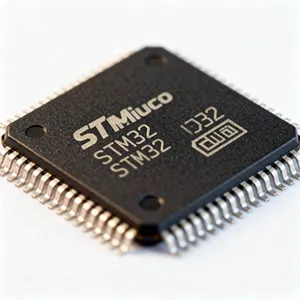
Through-Hole Packages
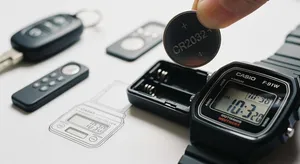
DIP
The Dual Inline Package (DIP) stands as one of the most recognized through-hole IC packages. You will see DIP chips with two parallel rows of pins. These pins go through holes in the printed circuit board (PCB) and get soldered on the other side. DIP packages come in many sizes, such as DIP-8, DIP-14, and DIP-40, with the number showing how many pins the chip has. You can easily handle and insert DIP chips by hand, which makes them popular for learning, prototyping, and repair work.
Features
-
DIP packages have a rectangular plastic or ceramic body.
-
Each side of the package has a row of pins spaced 2.54 mm (0.1 inch) apart.
-
You can use DIP chips in sockets or solder them directly to the PCB.
-
The design allows for easy manual assembly and replacement.
-
DIP packages support both analog and digital ICs.
Note: DIP packages help you test and swap chips without special tools. This makes them a favorite for breadboarding and early design work.
Advantages
Technical documents highlight several advantages of DIP packages. You can find DIP chips from many vendors, which makes sourcing easy. The cost of DIP ICs is often similar to surface-mount devices. You can place and solder DIP chips by hand, so you do not need expensive machines. This makes DIPs great for students, hobbyists, and anyone working on small projects. If you need to repair or upgrade a device, DIP chips are easy to remove and replace. These features make DIPs a strong choice for education, prototyping, and legacy system maintenance.
Disadvantages
DIP packages also have some drawbacks. The large size of DIP chips limits how many pins you can fit in a small space. For example, a DIP-14 is much bigger than a modern QFN or BGA with the same number of connections. The long pins add extra capacitance, which can slow down signals and reduce performance in fast circuits. DIP packages do not work well for high-speed or high-density designs. You may also find that DIP chips take up more space on your PCB, which can increase the size and cost of your project.
Applications
-
Through-hole technology began in the 1940s and grew in the 1950s and 1960s with new tools and better PCBs.
-
You will still find through-hole packages in aerospace, automotive, and medical devices because they handle heat and vibration well.
-
DIP chips work well for high-power circuits and places where you need strong, reliable connections.
-
You can use through-hole components for prototyping and small-batch production. Manual assembly lets you adjust parts if the PCB is not flat.
-
Through-hole packages make it easy to test circuits and fix problems during development.
-
Many industries choose through-hole packages when they need durability and easy repair.
Tip: If you want a package that is easy to handle, strong, and simple to replace, DIP and other through-hole packages are a smart choice for your next project.
Surface-Mount Packages
Surface-mount packages are also called SMDs. They changed how people make electronics today. You do not need to drill holes in the PCB. Instead, you put these parts right on top of the board. This way, devices can be smaller and lighter. They can also be more powerful. You see surface-mount packages in almost every new gadget. They are in things like smartphones and medical tools.
SOP
The Small Outline Package, or SOP, is a common SMD type. SOP chips have two rows of gull-wing leads on the sides. These leads help machines place and solder the chip. SOP comes in sizes like SOP-8 or SOP-16. The number tells you how many pins it has. SOP is used for memory chips, logic ICs, and small microcontrollers.
SOIC
The Small Outline Integrated Circuit, or SOIC, looks like SOP. But SOIC has a thinner body and shorter leads. You use SOIC when you want a small design. It is easy for machines to put SOIC on the board. The gull-wing leads help with soldering and checking the chip. SOIC is used for analog ICs, op-amps, and interface chips.
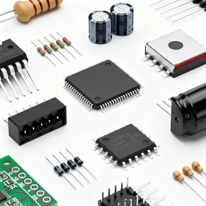
QFP
The Quad Flat Package, or QFP, has leads on all four sides. You use QFP when you need a chip with lots of pins. QFP comes in types like Thin QFP and Low-profile QFP. These help you fit big chips in small spaces. The leads are thin and close together. You need special machines to place and solder them.
QFN
The Quad Flat No-Lead, or QFN, has no leads you can see. Instead, there are metal pads under the chip. QFN is very small and handles heat well. You use QFN for fast and high-frequency circuits. It helps keep your design small and works well for signals. QFN is found in wireless chips, power ICs, and sensors.
SOT
The Small Outline Transistor, or SOT, is much smaller than other packages. SOT is used for transistors, diodes, and small ICs. SOT chips have three or more leads and take up little space. SOT-23 is often used in signal switching and voltage control.
Features
Surface-mount packages have many helpful features:
-
You can put parts on both sides of the PCB.
-
Short leads make circuits faster and more reliable.
-
Machines can place and solder SMDs quickly.
-
You can fit more parts in a small area.
Note: Surface-mount packages let you build complex circuits in small spaces. That is why they are in almost every new electronic device.
Advantages
Surface-mount technology, or SMT, has many good points:
-
Both sides of the PCB can hold parts, giving you more space.
-
Short leads mean better signals and less noise.
-
Machines place and solder SMDs fast, so labor costs go down.
-
You can make products that are smaller, lighter, and work better.
Here is a table that shows why surface-mount packages are growing in use and why companies like them:
|
Aspect |
Evidence |
|---|---|
|
SMT Market Size |
USD 4.5 billion in 2024, projected to reach USD 8.77 billion by 2032 (CAGR 8.5%) |
|
Adoption Drivers |
Growth in consumer electronics, electric vehicles, 5G, IoT, and medical devices |
|
Performance Enhancements |
Higher component density, miniaturization, automation, improved reliability |
|
Regional Trends |
Asia-Pacific leads in adoption; North America leads in advanced SMT for automotive, aerospace, defense |
|
Manufacturing Efficiency |
SMT reduces mechanical failures and increases reliability |
You can see that SMT is now the main way to make lots of fast, high-quality electronics.
Disadvantages
Surface-mount packages also have some problems:
-
Their small size makes them hard to handle and fix by hand.
-
You need special machines to place and solder them.
-
It is harder to check and test them because the leads are tiny or hidden.
-
Heat can build up if you put too many parts close together, so you must plan for cooling.
-
SMDs are not as strong as through-hole parts when things shake a lot.
Tip: Make sure your tools and skills are right for surface-mount assembly before you start.
Applications
You use surface-mount packages in almost every new electronic device. Here are some examples:
-
Phones, tablets, and laptops use SMDs because they are small and fast.
-
Medical devices need small, reliable circuits, so they use SMDs.
-
Cars use SMT for small, strong, and reliable electronics.
-
Aerospace and defense use SMDs for high-density, light designs.
-
Industrial IoT and 5G base stations use SMDs for fast data and small size.
SMT helps you in many ways:
-
You can make products that are smaller and lighter.
-
You can add more features to your designs.
-
You can build things faster and for less money.
-
You get better signals and more reliable devices.
Here are reasons why SMT is great for small electronics:
-
You do not need holes, so devices can be thinner.
-
Both sides of the PCB can have parts.
-
Machines make building faster and cheaper.
-
You can fit more features in a small space.
Note: Surface-mount packages help you keep up with the need for smaller, faster, and smarter devices.
Pin Grid Array Packages
PGA
Pin Grid Array (PGA) packages have many pins on the bottom. These pins are in a grid shape. You can plug the pins into a socket or solder them to a board. This makes it simple to change or upgrade chips. PGA is often found in old computers and some microprocessors. The pins stick out and can bend, so you must be careful.
BGA
Ball Grid Array (BGA) packages use tiny solder balls instead of pins. The balls are in a grid under the chip. When you heat the board, the balls melt and connect the chip. BGA lets you fit more connections in a small area. You see BGA in new CPUs, GPUs, and memory chips. The solder balls help move heat away and keep the chip cool.
Features
|
Metric / Aspect |
Value / Detail |
Impact / Significance |
|---|---|---|
|
Pin Count |
Very high number of connections in a small space |
|
|
Solder Ball Pitch |
Down to 0.25 - 0.4 mm (MicroBGA) |
Small spacing makes design harder |
|
Connection Path Length |
0.8 to 1.2 mm |
Short paths mean less signal loss |
|
Electrical Parameters |
Inductance: 0.5–2.0 nH; Capacitance: <0.1 pF |
Good for fast signals and less unwanted effects |
|
Thermal Resistance (JA) |
14.9°C/W (Cavity PBGA), 17.9°C/W (Overmold PBGA) |
Helps get rid of heat in strong chips |
|
Junction Temperature |
~100°C (Cavity PBGA at 3.8W), ~110°C (Overmold PBGA at 3.8W) |
Keeping chips cool is very important |
|
PCB Design Constraints |
Fine pitch routing, via-in-pad, blind/buried vias, increased layer count |
Makes building the board harder and costs more |
|
Inspection Methods |
X-ray inspection required |
X-rays check for problems you cannot see |
Advantages
-
PGA and BGA can have lots of pins.
-
BGA gives better signals because paths are short.
-
Solder balls in BGA help cool the chip.
-
PGA is easy to fix or swap because pins are easy to reach.
Note: BGA can send data very fast, up to 56 Gbps, with little signal loss. This is great for strong devices.
Disadvantages
-
PGA pins can bend or break if you are rough.
-
BGA is hard to fix because you cannot see the joints.
-
You need special tools like X-rays to check BGA chips.
-
Small spacing and many pins make boards harder and cost more.
Applications
You find PGA and BGA in many big devices:
-
CPUs and GPUs in computers and servers
-
Fast memory chips
-
Network switches and routers
-
Game consoles and graphics cards
BGA is good for things that need many connections and fast signals. PGA is still good if you want to change chips easily.
Other Notable Packages
PLCC
You may see the Plastic Leaded Chip Carrier (PLCC) in many older and some current electronics. PLCC uses a square or rectangular plastic body with leads bent underneath. These leads help you mount the chip on the surface of the PCB. PLCC packages allow you to use sockets or solder them directly. This makes them flexible for both prototyping and production. The leads molded into plastic make the package strong, but you might find it hard to inspect the solder joints after assembly.
CSP
Chip Scale Package (CSP) stands out for its small size. The package is only a little bigger than the chip itself. CSPs fit well in devices where space matters, like smartphones and tablets. You can use CSPs when you want to save space and reduce weight. The compact design helps you build thinner and lighter products. CSPs also support high-speed signals because the connections are short.
WLP
Wafer Level Package (WLP) is one of the most advanced types. You get a package that is almost the same size as the chip. Manufacturers finish the packaging steps while the chip is still part of the wafer. WLPs are very thin and light. You can use them in products where every millimeter counts. WLPs also cost less to make because the process is efficient. The use of materials like copper and special plastics helps keep the package strong and reliable.
Features
-
PLCC lets you mount chips on both sides of the PCB.
-
CSP and WLP offer very small and thin profiles.
-
WLP gives you the best die-to-package ratio.
-
All three types help you save space on your board.
Note: You can use these packages to make your designs smaller and lighter.
Advantages
-
PLCC is easy to handle and works with sockets.
-
CSP fits in tight spaces and supports fast signals.
-
WLP is thin, light, and cost-effective.
-
You can mount these packages on both sides of the PCB.
Disadvantages
-
PLCC makes it hard to check solder joints.
-
CSP and WLP can have problems with heat and stress.
-
WLP may face thermal mismatch issues in some cases.
-
You need special tools to inspect and repair these packages.
Applications
You find PLCC in older computers, industrial controls, and some telecom gear. CSP and WLP are common in mobile phones, tablets, and wearables. You also see them in cameras and other small gadgets. These packages help you build products that are small, light, and full of features.
Choosing the Right IC Package
Electrical Performance
You should think about electrical performance first. The right package helps your circuit work better and faster. Some packages, like Flip-Chip Ball Grid Array (FC-BGA), give strong signal quality. They use short paths, so signals move quickly with less loss. Ball Grid Arrays (BGA) also help your circuit run fast and keep signals clean. Surface Mount Technology (SMT) packages let you put more parts in a small space. This cuts down on unwanted effects and makes things work better. Through-hole packages can be better for blocking outside signals because they have longer paths. The materials, number of pins, and how you mount the package all change how your circuit works.
-
FC-BGA: High speed, short paths, good for fast devices
-
CSP: Small, works well, but does not cool as much
-
LGA: Many pins, stable, helps with heat control
Tip: Always pick a package that fits your speed and signal needs.
Thermal Management
You need to control heat in your design. Good heat control keeps your device safe and working well. Tests show that a boiling-driven heat spreader with dot supports can keep the chip temperature difference as low as 7.6°C at high power. A solid copper heat spreader shows a bigger difference of 28°C. This means new heat spreaders help spread heat better and stop hot spots. Good heat transfer at high power keeps your device from getting hurt. When you pick a package, look for ways to move heat away from the chip.
Footprint and Pin Count
You should check the footprint and pin count before picking a package. The number and place of pins change how you design your board. Packages with many pins, like BGA, can have up to 1000 pins and be as big as 50-60 mm. Packages with fewer pins, like QFN or WLCSP, are smaller but may not cool as well. The layout matters too. If the I/Os are on the edge, wire bonding works well. If they are spread out, flip chip packaging is better.
|
Aspect |
Details |
|---|---|
|
Pin Count |
Number and place of I/O pins matter a lot |
|
High Pin Count |
BGA; up to 1000 pins; large size (50-60 mm) |
|
Low Pin Count |
QFN or WLCSP (~50 pins); WLCSP cools less; QFN is better for grounding |
|
Layout |
Edge I/Os for wire bonding; spread out I/Os for flip chip packaging |
-
Pick a package that fits your I/O needs
-
Plan for adding more pins later
-
Think about how you will connect signals and power
Manufacturing Compatibility
You want your package to work with your way of building things. Surface-mount packages are good for machines and fast assembly. Through-hole packages are easier to put in by hand and fix. You need to set pad size, shape, and spacing the right way. Use the right names and points for machines to find. Picking the right footprint stops problems when building. Sometimes, you need special footprints for unique parts.
Note: Picking the right package helps you avoid mistakes and makes your product easier to build.
Summary of Essential IC Package Types
You have learned about the most important IC package types in electronics. Each type has its own shape, size, and way of connecting to a circuit board. When you pick a package, you decide how your device will look, how well it will work, and how easy it will be to build.
IC packages have changed a lot over time. At first, you saw through-hole packages like DIP and PGA. These were big and easy to handle. Later, surface-mount packages like QFP and QFN became popular. These let you make smaller and faster devices. Now, you see area array packages like BGA and advanced types like CSP and WLCSP. These new packages help you fit more power into less space.
Here is a table that shows how IC packages have evolved and what makes each family special:
|
IC Package Families |
Key Characteristics |
Evolution Stages |
Statistical Highlights |
|---|---|---|---|
|
QFP, PBGA, LGA, FCBGA |
Size, height, ball pitch, lead count, wafer size, stacked die, speed, power, reliability |
1st: Through-hole (DIP, SIP, PGA) |
LGA: 5x5 to 19x19 mm², height 1.2-1.4 mm, pitch 0.5-1.0 mm, up to 5 GHz, 10 Gbps, 4 W, Level 3 reliability |
|
High-density (CSP, Flip Chip) |
Small size and weight, better electrical performance, simpler boards |
Flip Chip use grew from 12% in 2010 to 20% in 2020 |
CSP area 13% of QFP, Flip Chip area 10% of QFP, CSP weight 20% of QFP |
Tip: When you choose from the Essential IC Package Types, think about your project’s needs for size, speed, and how easy it is to build and repair.
You can see that new packages let you build smaller, faster, and more reliable devices. You also get more choices for power and speed. By understanding these types, you make better decisions for your designs.
You should learn about Essential IC Package Types before you design. The package you pick changes how your device works and how simple it is to make. Always look at datasheets and ask experts for advice. Groups like ESDA say this helps you follow new rules and avoid problems.
Keep asking questions—market news and articles show that packaging changes quickly. Keep learning so your designs work well and stay current.
FAQ
What is the main difference between through-hole and surface-mount packages?
Through-hole packages have pins that go through holes in the PCB. Surface-mount packages sit on top of the board. You can use through-hole for strong connections. Surface-mount helps you save space and build smaller devices.
Why do you need to care about IC package size?
Package size affects how many parts you can fit on your board. Smaller packages let you make compact devices. Large packages are easier to handle but take up more space. Always check your design needs before you choose.
Can you solder surface-mount devices by hand?
Yes, you can solder some surface-mount devices by hand. Small packages like SOT-23 are possible with practice. Very tiny packages, like BGA, need special tools. You should use tweezers and a fine-tip soldering iron for best results.
How do you choose the right IC package for your project?
You should look at your design, speed, heat, and how you will build the device. Check the number of pins and the space you have. Always read datasheets and talk to experts if you feel unsure.