Designing High-Performance Integrated Circuit Boards: Best Practices and Industry Standards
Designing high-performance integrated circuit boards requires skill and careful planning. Every choice in the design impacts how well the board functions. Utilizing best practices and guidelines contributes to creating superior boards.
Designing high-performance integrated circuit boards requires skill and careful planning. Every choice in the design impacts how well the board functions. Utilizing best practices and guidelines contributes to creating superior boards. For instance, adhering to IPC rules minimizes errors and enhances part compatibility. It also simplifies the assembly of the boards. By following these guidelines, you can improve the performance of your high-performance integrated circuit boards and increase sales. These standards assist engineers in producing boards that meet global benchmarks and operate reliably.
Key Takeaways
-
Use IPC rules to make PCBs better and avoid mistakes. These rules help PCBs work well and fit with other parts.
-
Keep signals clear by matching trace lengths and controlling impedance. This helps data stay accurate and avoids communication problems.
-
Manage heat with tools like thermal vias and heat sinks. Good heat control makes PCBs last longer and stops damage.
-
Test your designs early by making prototypes. Prototyping finds problems before production, saving time and money.
-
Try simulation tools to check PCB designs on a computer. These tools spot issues and improve designs before building them.
Basics of High-Performance PCB Design
What Are Printed Circuit Boards?
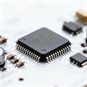
Printed circuit boards (PCBs) are the base of electronics today. They connect and hold electronic parts using copper pathways and pads. PCBs have changed a lot over the years.
-
In 1903, Albert Hanson invented through-hole construction, still used now.
-
By 1941, Paul Eisler made the first working PCB, sold in 1948.
-
The 1980s brought surface mount technology, making smaller, better designs.
-
Newer methods, like 3D printing, have changed PCB design even more.
These changes show the need for smaller, faster circuit boards in many industries.
Important Features of High-Performance PCBs
High-performance PCBs have key features that make them work well. These features help them last longer and perform better in tough conditions.
|
Feature |
What It Does |
|---|---|
|
Keeps signals clear with low loss and distortion. |
|
|
Stops overheating by spreading heat evenly. |
|
|
Strength |
Makes sure the board doesn’t break when bent. |
|
Layer Bonding |
Keeps layers stuck together under stress. |
|
Heat Transfer |
Moves heat away to protect components. |
|
Material Expansion |
Prevents cracks by matching material expansion rates. |
These features make these PCBs great for industries like space and communication.
How Design Choices Affect PCB Performance
The way you design a PCB changes how it works. For example, bad trace paths can mess up signals, and poor heat control can cause overheating. Engineers must focus on important performance areas during design:
|
Area |
Why It Matters |
|---|---|
|
Signal Quality |
Keeps data clear by matching trace length and impedance. |
|
Power Flow |
Reduces voltage drops with capacitors and power planes. |
|
EMI Control |
Lowers interference with shielding and smart layouts. |
|
Heat Control |
Stops overheating with heat sinks and thermal vias. |
By focusing on these areas, you can make PCBs that work well and last long. This ensures they meet the needs of today’s advanced electronics.
Industry Standards for High-Performance PCBs
IPC Standards and Their Role
IPC standards help make printed circuit boards (PCBs) reliable and high-quality. These rules, created by the Association Connecting Electronics Industries, guide every step of PCB creation, from design to production. By using IPC standards, you can avoid mistakes and get better results.
One popular standard is IPC-2221, which gives tips for PCB design. It helps you choose the right materials and trace sizes to improve performance. Another key standard, IPC-A-610, checks if electronic assemblies meet high-quality levels. This ensures your boards work well even in tough conditions.
Using IPC standards also makes teamwork between engineers and manufacturers easier. When everyone follows the same rules, communication improves, and production becomes faster. Studies show these standards can cut production time by 30% and boost success rates to 95%.
ISO Certifications for PCB Quality
ISO certifications prove that your PCBs meet global quality standards. These certifications, given by the International Organization for Standardization, cover quality control and eco-friendly practices.
ISO 9001 is a common certification for PCB makers. It focuses on keeping processes consistent to deliver reliable products. Having this certification builds customer trust and helps you compete in the market.
ISO 14001 focuses on protecting the environment. It encourages reducing waste, saving energy, and using green methods. About 40% of PCB factories now follow ISO 14001, showing the industry's focus on sustainability.
|
Certification |
Focus Area |
Benefits |
|---|---|---|
|
ISO 9001 |
Quality Management |
Ensures consistent product quality |
|
ISO 14001 |
Environmental Sustainability |
Promotes eco-friendly manufacturing |
RoHS Compliance and Environmental Considerations
RoHS compliance is important for making safe and eco-friendly PCBs. The Restriction of Hazardous Substances (RoHS) rule limits harmful materials like lead and mercury in electronics. Following these rules helps you create safer products.
RoHS compliance also makes your products more marketable. Many countries require RoHS standards for electronics to be sold. By making RoHS-compliant PCBs, you can reach more customers who care about the environment.
You should also think about other green practices when designing PCBs. For example, using recyclable materials and saving energy during production can help. Over the last 10 years, the number of PCB factories following green rules has grown from 25% to over 70%, showing a big move toward eco-friendly practices.
Best Practices in PCB Design
Optimizing Layer Stack-Up
Arranging layers properly is key for better PCB performance. It helps signals stay clear, reduces EMI, and manages heat well. A good layer stack-up also follows IPC standards, ensuring reliability and meeting rules.
To design a strong layer stack-up, follow these tips:
|
Aspect |
Description |
|---|---|
|
Signal Layers and Return Planes |
Pair each signal layer with a nearby return plane. |
|
Coupling |
Keep signal layers close to their return planes. |
|
Power and Ground Planes |
Place power and ground planes together for better capacitance. |
|
High-Speed Signals |
Route fast signals on inner layers to avoid interference. |
|
Multiple Ground Planes |
Use extra ground planes to lower inductance. |
|
Critical Signal Routing |
Limit key signal paths to two layers with the same reference plane. |
These steps improve performance and make fixing issues easier. For example, capped vias in stack-ups allow 6.2% more circuit density. They also lower short circuit risks by 14%. By using these methods, you can build reliable, high-performance PCBs.
Ensuring Signal Integrity
Good signal integrity keeps PCBs working smoothly. Bad signal quality can cause data errors and system problems. To keep signals strong, focus on routing, impedance, and reducing noise.
Here are simple ways to protect signal integrity:
-
Match Trace Lengths: Make trace lengths equal for paired signals.
-
Control Impedance: Keep trace widths and spacing consistent.
-
Minimize Crosstalk: Space out traces and use ground planes to separate signals.
-
Reduce Noise: Add capacitors near power pins to filter noise.
Using these ideas improves PCB performance. For instance, filled vias last 2.8 times longer in thermal cycles than unfilled ones. This boosts signal quality and makes PCBs last longer.
Effective Power Distribution Network Design
A steady power network is crucial for PCB function. It ensures all parts get stable power, avoiding errors. Focus on materials, capacitor placement, and strong metal connections.
Important PDN needs include:
|
Requirement |
Description |
|---|---|
|
Use enough metal to connect power sources and parts. |
|
|
Capacitor Specifications |
Pick the right size, value, and number of capacitors. |
Follow these extra tips for PDN design:
-
Use materials with a Tg above 160°C, like EM-528 or Ventec VT-447 FR4.
-
Choose larger vias, such as a 0.031-inch hole and 0.050-inch pad, for better current flow.
-
Select a HASL finish with a 62:38 tin-to-lead ratio for easier soldering.
By following these steps, you can create a PDN that meets PCB standards. A good PDN improves performance, lowers costs, and makes maintenance simpler.
Managing Thermal Performance
Keeping PCBs cool is important for making them last longer. Too much heat can harm parts, mess up signals, or even break the system. Using good heat control methods helps your PCBs work better and follow IPC standards.
Why Heat Control Is Important
Electronics always produce heat when they work. If heat builds up, it creates hot spots that can damage parts or make them less efficient. Uneven heat can also cause cracks or layers to peel apart. This often happens during soldering, where fast heating can create stress and strain.
Ways to Manage Heat in PCBs
Here are some simple ways to handle heat in your PCB design. These tips help spread heat evenly and keep your board working well:
-
Add Thermal Vias: Put thermal vias near hot parts. They move heat to cooler layers below.
-
Pick Heat-Friendly Materials: Use materials that transfer heat well. This helps parts stay cool.
-
Place Parts Smartly: Keep heat-sensitive parts away from power-heavy ones. This improves airflow.
-
Use Heat Sinks: Attach heat sinks to hot parts. They absorb and spread heat to keep things cool.
-
Heat Slowly During Soldering: Gradual heating stops uneven stress and prevents damage.
Tools to Check Heat Problems
Special tools can help you find heat issues before building your PCB. Software lets you see how heat moves and find problem areas. These tools help you choose the right materials, layer setup, and part placement.
|
Heat Control Method |
What It Does |
|---|---|
|
Thermal Vias |
Moves heat between PCB layers. |
|
Heat-Friendly Materials |
Helps parts stay cool at key spots. |
|
Heat Sinks |
Absorbs and spreads heat from hot parts. |
|
Smart Part Placement |
Lowers stress and improves airflow. |
Why Good Heat Control Helps
Using these methods makes your PCBs stronger and more reliable. Good heat control stops parts from breaking, keeps signals clear, and meets IPC standards. It also saves energy and helps meet eco-friendly rules.
Tip: Test your PCB in real-world conditions to check its heat control. Stress tests can show hidden problems and confirm your design works well.
By focusing on heat control, you can build strong, high-performance PCBs that meet both technical and environmental needs.
Advanced Techniques for High-Performance PCB Optimization
High-Speed Design Strategies
Making PCBs for high-speed systems needs careful planning. You must keep signals clear and reduce losses. Focus on routing and layer arrangement to support fast digital systems. Pair signal layers with nearby ground planes to lower interference. Shorter traces also help signals stay strong and clear.
Check your design using important performance measures. These include signal-to-noise ratio (SNR), insertion loss, and return loss. Eye diagrams are useful too. They show signal quality visually. An open eye means the signal is good.
|
Metric |
What It Shows |
|---|---|
|
Signal-to-Noise Ratio |
Compares signal strength to background noise. |
|
Insertion Loss |
Shows how much signal weakens as it travels. |
|
Return Loss |
Measures signal reflection from mismatched impedance. |
|
Eye Diagram Analysis |
Displays signal quality; a closed eye means poor performance. |
Using these strategies helps your PCB work well for high-speed tasks while meeting industry rules.
Reducing Electromagnetic Interference
Electromagnetic interference (EMI) can harm PCB performance, especially in fast designs. To lower EMI, place capacitors near chips and board edges. This reduces radiation from power and ground layers. Shorter traces also cut down interference.
Studies show these methods work well. Capacitors near chips reduce radiation a lot. Shielding and filtering also help lower emissions.
|
Method |
How It Helps |
|---|---|
|
Capacitor Placement |
Reduces radiation when placed near chips and edges. |
|
Shorter traces lower electromagnetic interference. |
|
|
Shielding and Filtering |
Cuts down emissions with protective techniques. |
Using these ideas ensures your PCB meets high-performance needs and follows industry standards.
Leveraging Simulation Tools
Simulation tools are great for testing PCB designs before building them. They help find problems early and save time and money. You can test signal clarity, heat control, and EMI to meet design goals.
For fast designs, simulations check signal paths and improve routing and layer setup. They also test capacitor placement and trace routing to lower EMI. These tools make your PCB better and more reliable.
Tip: Use simulation software to see heat flow and signal paths. This helps you fix issues and improve your design.
Simulation tools are key for making strong, high-quality PCBs that follow industry rules.
Challenges and Solutions in PCB Design
Balancing Cost and Performance
Balancing cost and performance in PCB design takes careful planning. You need to check materials, manufacturing methods, and design details to save money. A detailed BOM (Bill of Materials) review can show where to cut costs. For example, choosing cheaper materials that still keep good signal quality and heat control can lower expenses without hurting performance.
To do this, focus on layout and use advanced design tools. These tools help improve signal paths, power flow, and heat control. This ensures your PCB works well without going over budget. Placing parts correctly during design also avoids delays and lowers production costs.
|
How It Helps with Cost and Performance |
|
|---|---|
|
Data Transparency |
Shows material availability and pricing clearly. |
|
Supplier Integration |
Makes it easy to use supplier data in designs. |
|
Enhance Design Efficiency |
Adjusts designs quickly based on available parts. |
|
Reduce Costs |
Avoids extra costs from last-minute changes. |
By focusing on these areas, you can make PCBs that are affordable and reliable.
Addressing Design Complexity
Complex PCB designs can be tricky, but smart solutions make them easier. Focus on keeping signals strong by using impedance matching and routing traces carefully. Advanced testing tools, like flying probe testers, find problems early and save time.
Here are some real-life examples of solving design challenges:
-
FCT fixed a flexible circuit design for a customer, solving issues and making great prototypes.
-
A customer needed a flat thermal sensor design. FCT improved it, leading to smooth production.
-
Company B used AI tools to check quality, cutting defects by a lot.
These examples show how creative ideas can handle complex designs while keeping them fast and easy to build.
Ensuring Manufacturability
Making PCBs easy to manufacture is key for good results. Check via sizes, trace widths, and spacing to match manufacturer rules. For instance, keeping a thickness-to-via ratio of 8:1 helps make strong connections.
|
Design Aspect |
What to Do |
|---|---|
|
Thickness-to-via ratio |
Use 8:1 for strong hole connections. |
|
Trace width |
Use 0.05mm for HDI PCBs. |
|
Via sizes and spacing |
Check sizes and keep proper spacing. |
Doing manufacturability checks early avoids delays and fixes. Modern tools like ICT systems help find problems faster and improve control. By planning for manufacturability, you can make production smoother and improve PCB quality.
Tip: Work with your manufacturers to adjust designs for easier production. This saves money and ensures your PCB meets industry rules.
Testing and Validation of High-Performance PCBs
Prototyping for Design Validation
Prototyping helps ensure your PCB works as planned. By making prototypes, you can test designs early and find problems before production. This saves both time and money while improving the board's quality.
Benefits of prototyping include:
-
Cost Efficiency: Fixing problems in prototypes costs less than fixing them later.
-
Better Reliability: Testing prototypes in different conditions ensures they work in real life.
-
Finding Design Errors: Early prototypes reveal mistakes, helping you improve the design.
For example, a medical startup used modular prototypes for a diagnostic device. They found 37 design issues, launched eight months faster, and saved $250,000. Prototyping makes your PCB stronger and speeds up development.
Electrical Testing Methods
Electrical tests check if your PCB works properly. These tests look at power flow, signals, and overall performance. They ensure your PCB meets standards and works reliably.
Common electrical tests include:
-
Functional Testing: Checks if the PCB does its basic tasks.
-
Electrical Testing: Uses tools to measure power and signal flow.
-
Reliability Testing: Tests how the PCB handles stress like heat or pressure.
-
Thermal Testing: Examines how the PCB works in extreme temperatures.
These tests give useful feedback about your PCB's performance. They help you deliver a reliable, high-quality product.
Environmental Stress Testing
Environmental stress tests check how your PCB handles tough conditions. These tests make sure your design can survive heat, moisture, and vibrations. Simulating real-world conditions helps find weak spots and improve durability.
Key stress tests include:
-
Thermal Cycling: Tests how the PCB handles quick temperature changes.
-
Humidity Testing: Checks how moisture affects the PCB's function.
-
Vibration Testing: Simulates shaking to ensure the PCB stays intact.
These tests help you build a strong PCB that meets standards and works well in harsh environments.
Using best practices and industry standards helps your PCB designs work well. Following these rules makes boards reliable and meet global goals. Tools like simulation software and prototypes help fix problems early. Improving your design process keeps your boards modern and ready for new tech.
Tip: Check industry standards often and try new tools to improve your PCB designs.
FAQ
What matters most in high-performance PCB design?
Keeping signals clear is the most important part. It helps parts communicate without problems. To do this, match trace impedance, reduce signal mixing, and use good grounding. These steps make your PCB work better and last longer.
How do rules like IPC help with PCB design?
Rules like IPC give clear steps for making PCBs. They guide you on materials, design, and building methods. Following these rules lowers mistakes, improves part matching, and makes boards more reliable.
Why is heat control important in PCB design?
Heat control stops parts from getting too hot and breaking. You can manage heat by adding special holes, using heat sinks, and picking materials that handle heat well. This keeps your PCB safe and working properly.
How do design tools help improve PCBs?
Design tools let you test your PCB on a computer first. They show problems with signals, heat, or interference before building. This saves time and ensures your PCB works as planned.
Why is testing a prototype useful in PCB design?
Testing a prototype helps you find and fix mistakes early. It makes your PCB stronger, more reliable, and cheaper to produce. Fixing problems in the prototype stage avoids expensive changes later.