Critical Steps in the PCB Board Assembly Process for Electronic Manufacturing
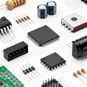
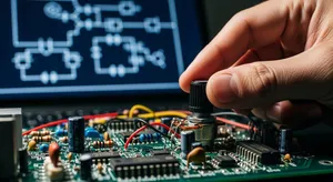
The PCB board assembly process transforms a bare printed circuit board into a working electronic device. You start by applying solder paste, then place components on the board. Next, the assembly moves to soldering, inspection, and testing. Precision and quality matter at every stage.
The PCB board assembly process transforms a bare printed circuit board into a working electronic device. You start by applying solder paste, then place components on the board. Next, the assembly moves to soldering, inspection, and testing. Precision and quality matter at every stage. Recent industry recalls show that mistakes in the process can cause safety risks and high costs. Automated machines and manual methods both play a role, but automation now places components faster and detects defects more reliably. Strict standards help ensure that each printed circuit board meets high quality and performance needs.
Key Takeaways
-
Start PCB assembly with precise solder paste application to ensure strong and reliable connections.
-
Use automated machines and skilled workers for fast, accurate component placement and soldering.
-
Choose the right soldering method—reflow for small parts, wave for through-hole components, and selective for mixed boards—to improve quality.
-
Inspect every board using AOI, X-ray, and visual checks to catch defects early and maintain high standards.
-
Prevent common defects like solder bridges and cold joints by following best practices and regular testing throughout the process.
PCB Board Assembly Steps
Solder Paste Application
You begin the pcb assembly process with solder paste printing. This step places small amounts of solder paste onto the pads of the printed circuit board. At NOVA PCBA, you work with partners who have delivered consistent quality for over ten years. You use advanced controls to make sure each deposit is precise. Good solder paste application is critical for the rest of the pcb board assembly process.
You can check the quality of solder paste printing by looking at several key points:
-
Print and pause data show how well the paste transfers over time.
-
You measure solder paste volume and area coverage to avoid weak joints or bridging.
-
You check the height and shape of each deposit for uniformity.
-
You use 3D inspection systems to spot problems early.
|
Parameter |
Description |
Importance |
|---|---|---|
|
Solder Paste Volume |
3D measurement of paste on pads |
Ensures strong solder joints |
|
Area Coverage |
How much of the pad has solder paste |
Prevents poor connections |
|
Alignment (X, Y, θ) |
Position and rotation of paste |
Helps with correct component placement |
|
Bridging and Separation |
Checks for unwanted connections |
Prevents shorts |
You also store solder paste in cool places and warm it up before use. You clean stencils often to keep the process stable. These steps help you keep the pcb assembly process reliable.
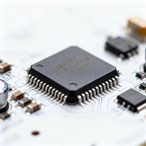
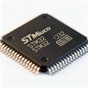
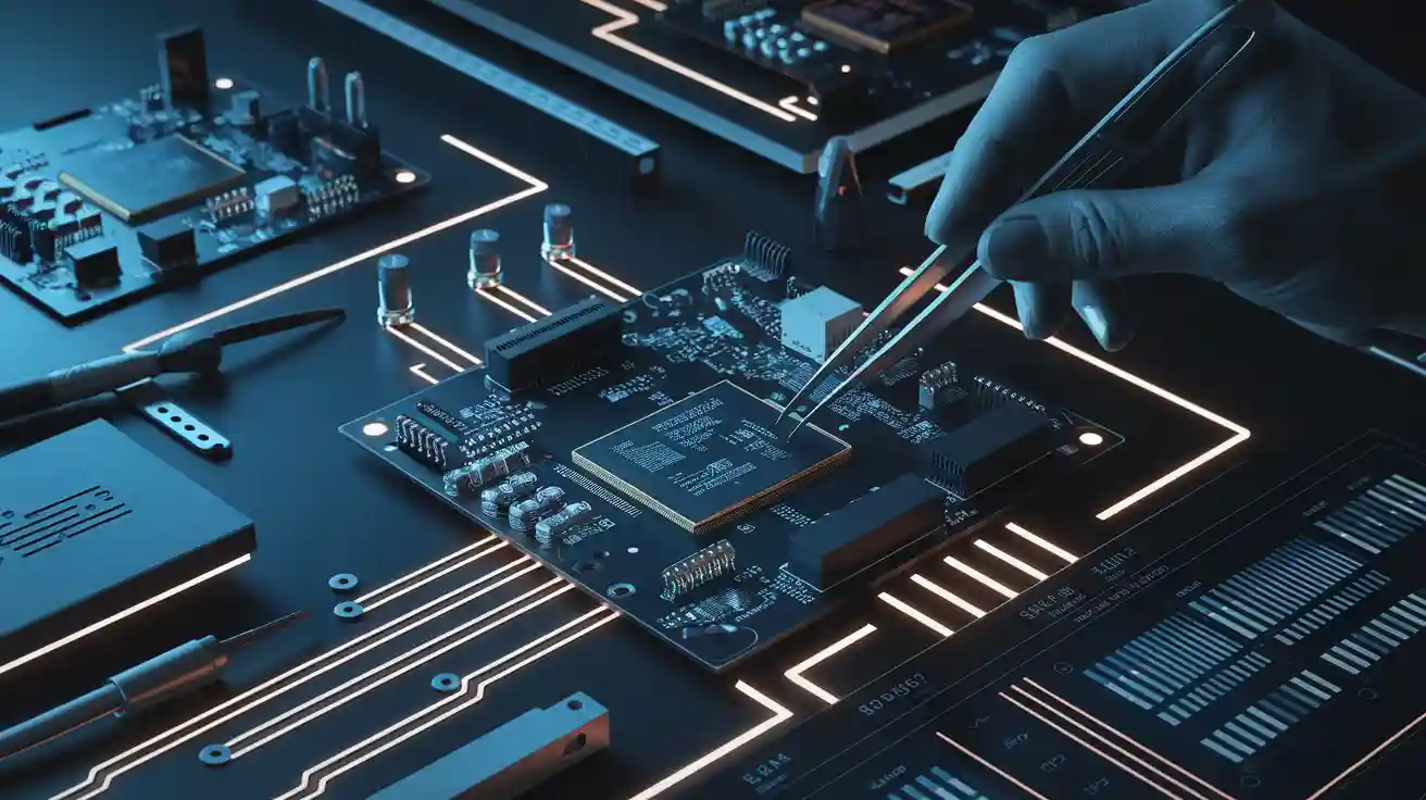
Component Placement
Next, you move to component placement. You use both machines and skilled workers to put each part on the printed circuit board. NOVA PCBA uses a strong supply chain to make sure every part is real and high quality. Automated pick-and-place machines work fast for large jobs. For special projects, you may place some parts by hand. This step turns the bare pcb into a real circuit.
Soldering
After placing the components, you start the soldering step. At NOVA PCBA, you work with engineers from top companies and trusted factories. You use both automated and manual soldering methods. This part of the pcb assembly process connects each part to the board. Good soldering gives you strong electrical and mechanical connections. Careful soldering helps you avoid defects and keeps the printed circuit board working well.
Tip: Always check your solder joints for smoothness and shine. Dull or cracked joints can cause problems later.
The pcb board assembly process changes a simple pcb into a working electronic device. Each step builds on the last, and your focus on quality ensures a reliable result.
PCB Assembly Process Methods
Surface Mount Technology (SMT)
You use Surface Mount Technology (SMT) in the pcb assembly process when you want speed and accuracy. SMT places components directly onto the surface of the printed circuit board. Automated machines can place up to 120,000 parts per hour. These machines reach placement accuracy as fine as ±0.015mm. This allows you to use very small components and fit more on each pcb. SMT also helps you reduce errors. You can track quality with real-time data and spot problems early. SMT supports 24/7 production, so you can keep the assembly process moving without breaks. You also save money because you need less rework and fewer warranty claims.
-
SMT benefits:
-
High-speed placement
-
Handles tiny components
-
Reduces defects
-
Supports large-scale production
-
Tip: Use SMT for products that need to be small, fast, and reliable.
Through-Hole Technology (THT)
Through-Hole Technology (THT) is another method you use in the pcb assembly process. You insert component leads through holes in the printed circuit board and solder them on the other side. THT gives you strong mechanical bonds. This makes it a good choice for parts that face stress, like connectors or heavy components. THT often needs more manual work, so it takes longer than SMT. You may use THT when you want extra strength or when the design does not allow for surface mounting.
-
THT advantages:
-
Strong physical connections
-
Good for high-stress parts
-
Useful for some special components
-
Mixed Technology
Sometimes, you need both SMT and THT in the same pcb assembly process. Mixed Technology lets you combine the best features of each method. You use SMT for most parts to keep the printed circuit board small and efficient. You use THT for parts that need extra strength. This approach helps you build complex devices that need both high performance and durability. Mixed Technology also supports market growth by allowing you to design versatile products.
You can see that the pcb assembly process becomes more flexible with mixed technology. You get the speed and density of SMT and the strength of THT. This combination helps you meet different design needs and improve the overall quality of your assembly.
Soldering Techniques
Soldering creates both electrical and mechanical connections on your printed circuit board. You choose the right soldering method based on the type of components and the needs of your pcb assembly process. Each technique offers unique benefits for different assembly applications.
Reflow Soldering
You use reflow soldering most often for surface mount technology (SMT) in the pcb assembly process. In this process, you first apply solder paste to the pads on your pcb. Then, you place the components and heat the board in a controlled oven. The solder melts and forms strong joints. Reflow soldering works well for high-density boards and small parts.
Note: Reflow ovens use precise temperature profiles to avoid damaging sensitive components.
Statistical studies show that reflow soldering gives you consistent results. For example:
-
Engineers use finite element modeling to predict joint temperature and strength.
-
X-ray imaging checks for voids and defects in solder joints.
-
Data-driven changes to solder paste or oven settings can reduce defects and improve reliability.
|
Statistical Evidence Aspect |
Description |
|---|---|
|
Sample Size |
70 assemblies analyzed for reliability |
|
Process Control |
Single reflow recipe improves consistency |
|
Defect Analysis |
Statistical tests help identify and fix common issues |
Wave Soldering
Wave soldering is best for through-hole components in your pcb assembly process. You pass the printed circuit board over a wave of molten solder. The solder flows into the holes and connects the leads. This method gives you strong mechanical bonds, which are important for connectors and heavy parts.
|
Parameter / Factor |
Quantitative Effect / Finding |
|---|---|
|
Solder joint peak temperature >230°C |
|
|
Peak temperature >220°C |
100% vertical hole fill, no large voids |
|
Preheating temperature |
Improves hole fill and reduces voids |
|
Supports optimal soldering and defect reduction |
|
|
Nitrogen atmosphere |
Prevents oxidation, improves solder quality |
You can adjust the temperature and speed to get the best results. Nitrogen helps prevent oxidation and keeps your solder joints clean.
Selective Soldering
Selective soldering helps you work with complex boards that mix SMT and through-hole parts. You use this method when you need to solder only certain areas of the pcb. Mini solder waves or drop-jet nozzles apply solder with high precision.
-
You control temperature profiles to protect sensitive parts.
-
Nitrogen blanketing prevents oxidation.
-
You use real-time monitoring to keep the process stable.
-
Selective soldering reduces waste and thermal stress.
This technique lets you create intricate connections without damaging other components. You can also rework only the areas that need fixing, which saves time and materials.
Tip: Always match your soldering method to your assembly needs for the best quality and reliability.
PCB Inspection
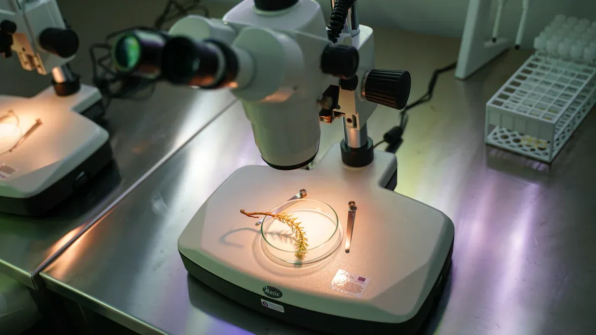
You need to check every pcb after the main pcb assembly process. Inspection helps you find problems early and keep the quality high. You use different inspection methods to make sure each pcb meets strict standards.
Automated Optical Inspection (AOI)
Automated Optical Inspection, or AOI, uses cameras and smart software to scan your pcb for defects. AOI systems work much faster than people and never get tired. You can spot tiny defects, even as small as 0.01 mm², which are hard for the human eye to see. AOI uses high-definition cameras and special lighting to catch issues like missing parts, wrong polarity, or solder bridges. Machine learning models in AOI systems can reach up to 99% accuracy for certain defects, such as polarity errors. This high accuracy means you get fewer false alarms and less wasted time. AOI also keeps inspection quality steady, while human inspectors may miss things if they get tired. You can see the difference in this table:
|
Metric |
AOI System Performance |
Manual Inspection Performance |
Improvement |
|---|---|---|---|
|
Precision |
Detects defects as small as 0.01 mm² |
Detects defects down to 0.1 mm² |
10 times more precise |
|
Speed |
Inspects 20 boards per minute (dual-lane) |
Inspects 0.3 boards per minute |
66 times faster |
|
Consistency |
Process capability index (CpK) ≥ 1.67 |
CpK ≤ 1.0 |
Yield improvement up to 40% |
AOI helps you catch problems early, reduce rework, and improve overall product quality.
X-ray Inspection
You use X-ray inspection when you need to see inside your pcb. This method finds hidden problems like voids, cracks, or bad solder joints that you cannot see from the outside. X-ray inspection uses both 2D and 3D imaging. With 3D CT scans, you can look at the inside of the assembly in great detail. X-ray inspection works fast and does not damage your pcb. You can check parts like BGAs and QFNs, which have hidden connections. This process helps you prevent failures and keep your assembly quality high.
Visual Inspection
Visual inspection means you or a trained worker look at the pcb with your eyes or a magnifier. You check for obvious problems, such as missing parts, wrong placement, or poor solder joints. Visual inspection works best for simple boards or as a final check after other tests. You should use visual inspection along with AOI and X-ray to make sure you do not miss any defects. This step adds another layer of quality control to your pcb assembly process.
Functional Testing
In-Circuit Testing
You use In-Circuit Testing (ICT) to check each part of your pcb after the main pcb assembly process. ICT helps you find problems early by measuring electrical values at special test points. You can spot issues like open circuits, short circuits, or wrong parts. ICT works fast and gives you clear pass or fail results for each board.
-
ICT measures voltage, resistance, and capacitance at test points.
-
You set pass/fail rules to decide if each part works as it should.
-
Test reports show problems like open circuits, shorts, wrong placement, weak solder joints, or parts with the wrong value.
-
The data from these tests tells you how well ICT finds errors in your pcb.
ICT covers many types of defects. You get quick and accurate results. Good contact and regular care of test pins help you get the best results. If you keep your ICT system in good shape, you can trust the data and improve your pcb assembly process.
Tip: Always check your test pins for wear. Clean pins give you more reliable test results.
Functional Testing
After ICT, you move to functional testing. This step checks if your pcb works as it should in real life. You run the board under normal conditions and measure things like voltage, current, and frequency. You see if the pcb meets all design needs.
-
Functional testing simulates real use and checks if the pcb does its job.
-
You can find problems that ICT might miss, such as system-level faults.
-
Sometimes, you see more failures at this stage if earlier tests missed something.
-
Fixing these problems can take more time and skill because they may involve several parts.
Functional testing lets you see if your pcb works for the customer. You do not need extra connections—just use the board’s own connectors. This method helps you find faults that only show up when the whole system runs. You can also use expert systems to help find and fix problems faster. By testing the pcb in real conditions, you make sure your product is safe and ready to use.
Note: Functional testing is your last line of defense before shipping. It helps you catch any hidden issues and ensures high quality.
Cleaning and Quality Control
Cleaning Process
You need to keep your pcb clean to ensure high quality and reliability. After each major step in the pcb assembly process, you should remove any residues or contaminants. Cleaning helps prevent problems like coating failures or electrical shorts. You can use several methods to check cleanliness:
-
Ion Chromatography (IC)
-
Resistivity Of Solvent Extract (ROSE) testing
-
Surface Insulation Resistance (SIR) testing
-
Visual inspection under UV light
-
Water contact angle measurement
You can measure the water contact angle before and after cleaning to see if the surface is ready for the next step. If you see residues, discoloration, or white powder, you know the pcb needs more cleaning. You should use temperature-controlled cleaning solutions and choose the right cleaning agents. Multiple cleaning cycles and precise timing help you get the best results.
|
Aspect |
Details |
|---|---|
|
Cleaning Process Standards |
Temperature-controlled solutions, optimized agents, timing, multiple cycles |
|
Efficiency Metrics & Quality Verification |
AOI, ionic contamination testing, SIR testing, cleanliness checks |
|
Cleanliness Testing Methods |
IC, SIR, contact angle, visual inspection under UV light |
|
Cleaning Frequency Recommendations |
Clean after each major step, especially post-soldering and pre-coating |
|
Visual Indicators for Cleaning Need |
Residues, discoloration, white powder, surface issues, high ionic contamination, low SIR, UV findings |
Design for Assembly (DFA)
You can make the pcb assembly process smoother by using Design for Assembly (DFA) practices. DFA means you design your pcb so it is easy to build and less likely to have errors. When you use DFA, you can reduce assembly time by up to 50% and cut production costs by up to 30%. Companies that use DFA often see fewer mistakes and better quality. You can use modeling tools to find where errors might happen and fix them before production starts. This approach helps you build reliable products and avoid costly rework.
Tip: Plan your pcb layout with DFA in mind to save time and improve quality.
Quality Assurance
You must check every pcb to make sure it meets strict quality standards. You can use several key performance indicators (KPIs) to track how well your process works. Here are some important ones:
|
KPI Name |
Description |
Relevance to Reliability |
|---|---|---|
|
First Pass Yield (FPY) |
Percentage of products passing all checks without rework. |
Shows process accuracy and efficiency. |
|
Defect Rate |
Percentage of defective units produced. |
Helps spot quality issues. |
|
Cycle Time |
Total time to assemble a product. |
Shorter times mean efficient processes. |
|
Throughput |
Number of units produced in a set time. |
Balances volume with quality. |
|
Overall Equipment Efficiency (OEE) |
Measures equipment availability, performance, and quality. |
Shows how well machines work. |
|
Rework and Repair Rate |
Percentage of products needing rework or repair. |
Lower rates mean better reliability. |
You should also follow standards like IPC-A-610 and ISO 9001. Use AOI, X-ray, and in-circuit testing to catch problems early. Keep good records for traceability. By following these steps, you make sure your pcb assembly process delivers high quality every time.
Common Defects
Solder Bridges
Solder bridges happen when extra solder connects two or more pads that should stay separate. This creates a short circuit. You often see solder bridges after reflow or wave soldering. Most solder bridges come from too much solder paste or poor stencil alignment. Automated Optical Inspection (AOI) helps you catch these defects early. Solder bridges can cause devices to fail or even overheat.
|
Defect Category |
Defect Rate (%) |
|---|---|
|
Quality defects related to solder paste printing |
|
|
Solder Shorts |
20 |
Tip: Always check for shiny, clean solder joints and watch for any unwanted connections between pads.
Cold Joints
Cold joints form when the solder does not melt completely or cools too quickly. You can spot a cold joint by its dull or grainy look. Cold joints make weak electrical connections. They often cause intermittent failures. You may see cold joints if the soldering iron is not hot enough or if the board moves during cooling. AOI and X-ray inspection help you find these defects before the pcb leaves the factory.
Misalignment
Misalignment means components do not sit in the right place on the pcb. This problem can happen if the board warps during manufacturing. When the board loses flatness, parts shift during reflow soldering. Misaligned parts can cause open circuits, short circuits, or even device failure. You need to keep the board flat and use fiducial markers for accurate placement. AOI and X-ray inspection help you spot misaligned parts and hidden defects.
-
Component misplacement and wrong orientation can cause short circuits and open circuits.
-
Soldering defects like bridges and cold joints often result from misalignment.
-
AOI uses cameras to find misplaced parts quickly.
-
X-ray inspection reveals hidden misalignments and solder voids.
Prevention
You can prevent most defects by following best practices at every step. Start with uniform solder paste application. Keep the paste at the right temperature and humidity. Use AOI and flying probe tests right after printing to catch errors early. Calibrate your machines and check them often. Control the reflow temperature to make sure solder joints form correctly. Use Standard Operating Procedures (SOPs) and update them as needed. Regular supplier audits and continuous improvement methods like Six Sigma help you reduce defects and improve efficiency. AOI, In-Circuit Testing, and functional testing all help you catch problems before the pcb reaches the customer.
Note: Good storage, ESD protection, and moisture control keep your boards safe and reliable.
You can achieve reliable results in the pcb assembly process by following each step with care. Inspection and testing, such as AOI and X-ray, help you catch defects early and improve quality. The table below shows how best practices boost performance:
|
Metric Category |
Key Indicators |
Purpose |
|---|---|---|
|
Quality Control |
Validates product quality |
|
|
Production Efficiency |
20% cycle time reduction |
Faster production |
|
Cost Management |
10-15% cost reduction |
Ensures cost efficiency |
-
Train your team and apply DFA principles.
-
Combine advanced inspection with functional testing.
Careful attention to each process step ensures your pcb meets high standards and delivers lasting performance.
FAQ
What is the main goal of the pcb board assembly process?
You turn a bare printed circuit board into a working device. The process connects each component to the board. You use steps like solder paste printing, placement, and soldering. Each step helps you build a reliable and high-quality assembly.
Why does solder paste printing matter in pcb assembly?
You need solder paste printing to hold components in place. Good printing gives you strong joints and fewer defects. If you skip this step or do it poorly, your assembly may fail. You improve quality by checking the paste before moving to the next process.
How do you make sure your pcb meets quality standards?
You use inspection tools like AOI and X-ray. You test each printed circuit board with in-circuit and functional tests. You follow strict process controls. You also clean the pcb after each step. These actions help you deliver high-quality assemblies.
Can you use both manual and automated methods in the pcb assembly process?
You can use both. Automated machines work fast and handle most parts. Skilled workers help with special or complex assemblies. You choose the best method for your project. This approach gives you flexibility and keeps your process efficient.
What are common defects in pcb board assembly and how do you prevent them?
You may see solder bridges, cold joints, or misalignment. You prevent these by using good solder paste printing, careful placement, and regular inspection. You also follow process guidelines and keep your workspace clean. These steps help you avoid defects and improve quality.