CD4040BF Explained: A Practical Guide to the 12‑Stage CMOS Ripple Counter
If you need a simple, wide‑voltage counter or frequency divider, the CD4040BF is a workhorse. In plain terms, it’s a CMOS 12
If you need a simple, wide‑voltage counter or frequency divider, the CD4040BF is a workhorse. In plain terms, it’s a CMOS 12‑stage binary ripple counter/divider with an asynchronous, active‑high reset—part of the classic CD4000 family—commonly offered in 16‑pin packages.
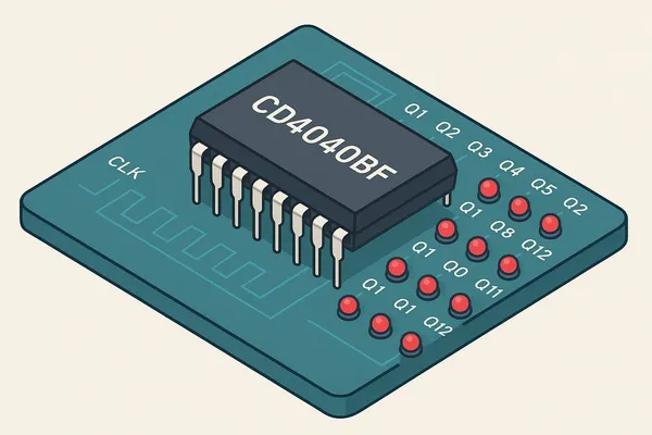
According to Texas Instruments’ device documentation, this class of device is a “12‑stage ripple‑carry binary counter” with a master reset that clears all outputs to 0, and it provides 12 divided outputs Q1 through Q12 as powers of two, i.e., fIN/2 … fIN/4096, as detailed in the TI CD4040B multi‑type datasheet (Rev. D, 2003). onsemi’s second‑source part confirms the same function and operating approach in the onsemi MC14040B datasheet PDF.
What the CD4040BF is—and is not
- Is: a CMOS ripple (asynchronous) counter/divider with 12 outputs and an active‑high asynchronous reset.
- Is not: a synchronous counter; the outputs don’t update simultaneously. It’s also not a microcontroller or programmable logic device.
Where the CD4040BF fits in your design
- Clock division: Derive slower clocks from a crystal or RC oscillator, from ÷2 up to ÷4096.
- Event counting: Count pulses from sensors or test equipment.
- Timing chains: Generate long delays by combining an oscillator with divided outputs.
- Frequency measurement: Build prescalers in measurement or monitoring setups.
Package and suffix: What “BF” usually means (and why to double‑check)
- In many catalogs, letters after “CD4040B” indicate package and environmental options. “BF” commonly maps to a plastic DIP or a specific SOIC/lead‑free variant depending on vendor lineage; however, these codes are not universal.
- Always verify the exact meaning of “BF” in the manufacturer’s ordering information and package tables for your chosen vendor and lot. TI publishes ordering and package details on the TI CD4040B product page, and timing/electrical characteristics in the TI CD4040B multi‑type datasheet.
Pinout and functional overview (conceptual)
- Inputs: CLOCK, RESET (asynchronous, active high).
- Outputs: Q1 (÷2), Q2 (÷4), …, Q12 (÷4096).
- Power: VDD and VSS (ground).
- Reset behavior: A high pulse on RESET clears all stages to 0 immediately, independent of CLOCK. See the timing/function description in the TI CD4040B multi‑type datasheet and corroborating tables in the onsemi MC14040B PDF.
Electrical characteristics snapshot (typical family behavior)
- Supply voltage (VDD): CD4000 devices run over a wide range. Vendors specify operation points around 5 V, 10 V, and 15 V, with absolute maximum VDD up to 18 V; consult the “Recommended operating conditions” and “Absolute maximum ratings” in the TI CD4040B multi‑type datasheet and the corresponding tables in the onsemi MC14040B datasheet PDF.
- Input thresholds: CMOS thresholds scale with VDD (roughly ~0.3×VDD for logic low max and ~0.7×VDD for logic high min); exact guaranteed levels are given per vendor in “Electrical characteristics” tables in the above datasheets.
- Maximum clock frequency: Increases with VDD and depends on load and temperature. Expect modest MHz capability at higher VDD and lower limits around the low‑voltage end; always check the timing/dynamic characteristics tables and curves in the TI CD4040B datasheet or onsemi’s PDF for your design point.
- Propagation/ripple: Because it’s a ripple counter, output changes propagate stage‑by‑stage, leading to short‑lived intermediate states. Factor this into any parallel decoding or timing that depends on multiple bits changing “at once” (see timing notes in the TI CD4040B datasheet).
How to use it: Frequency‑division examples
- Divide‑by‑N is built‑in: take the output from Qn to get fOUT = fIN/2ⁿ.
- Example 1: With a 32.768 kHz watch crystal as the input clock, Q12 outputs approximately 8 Hz (32,768 / 4096 ≈ 8). Handy for LED blinkers or low‑rate timers.
- Example 2: With a 1 MHz clock, Q10 outputs ~976.6 Hz (1,000,000 / 1024). Ensure your chosen VDD and loading meet the device’s frequency limits per the timing specs in TI/onsemi datasheets linked above.
- Reset usage: Apply a brief high pulse on RESET at power‑up to start from a known state; minimum reset pulse widths are specified in the timing characteristics of the TI CD4040B datasheet and the onsemi MC14040B PDF.
Design tips and common pitfalls
- Decouple the supply: Place a 0.1 µF ceramic capacitor close to VDD–VSS for stability; standard CMOS practice reflected in typical application recommendations in vendor datasheets.
- Condition slow or noisy clocks: If your input edge is slow or bouncy (e.g., mechanical switch), use a Schmitt‑trigger buffer (such as CD40106B) or proper debouncing before the counter; see general input characteristics guidance in the onsemi datasheet.
- Manage ripple hazards: Avoid combining multiple changing outputs directly for time‑critical logic. If you must decode multiple bits, latch them on the opposite clock edge or use a synchronous counter instead (timing behavior discussed in the TI datasheet).
- Unused pins: Tie unused inputs to defined logic levels; unused outputs can be left unconnected. Confirm any vendor‑specific notes in the electrical characteristics sections.
CD4040BF vs. 74HC4040 (when speed or 5 V logic matters)
- Function: Both are 12‑stage ripple counters with asynchronous reset.
- Voltage range: CD4040B family runs over a wide range typical of CD4000 CMOS (commonly 3–15 V operation points; see TI/onsemi), while 74HC4040 targets 2–6 V logic systems.
- Speed: 74HC4040 is much faster at 5 V—on the order of tens of MHz depending on load and conditions—per the Nexperia 74HC/HCT4040 datasheet (Feb 2024). Choose HC if you need higher speed within 5 V logic; choose CD4040B if you need wide‑voltage operation or low‑power CMOS across higher VDD.
Selection and sourcing notes
- Cross‑vendor equivalents include TI CD4040B, onsemi MC14040B/CD4040B, ST HCF4040B, and Nexperia HEF4040B. Match function, package, temperature grade, and environmental status.
- Suffixes like “BF” are vendor‑specific ordering codes. Confirm the exact package (PDIP, SOIC, TSSOP), tape‑and‑reel vs. tube, and RoHS/lead‑free status in the ordering information tables on the vendor’s product page—e.g., TI’s CD4040B product page—before placing an order.
Key references and further reading
- Device definition, pin functions, timing and electrical characteristics: see the TI CD4040B multi‑type datasheet (Rev. D, 2003).
- Second‑source data and timing tables: consult the onsemi MC14040B datasheet PDF.
- High‑speed 5 V comparison device: see the Nexperia 74HC/HCT4040 datasheet (Feb 2024).
By keeping the ripple nature, voltage range, and vendor‑specific ordering codes in mind—and by checking the linked datasheet tables—you can drop the CD4040BF into clock‑division and counting tasks with confidence.