7 Critical Steps in Electronic PCB Assembly: From Design to Final Testing
You need to pay attention to the critical steps that help your printed circuit board assembly work well. Every step in the PCB assembly process affects how good and reliable it is.
You need to pay attention to the critical steps that help your printed circuit board assembly work well. Every step in the PCB assembly process affects how good and reliable it is. If you plan early and think about PCB design, you can stop mistakes and save money on fixing problems. DFM and DFT are very important when getting ready for manufacturing. They help you find mistakes early, lower the number of failures by up to 50%, and make your product more reliable by 40%. When you use the right design for manufacturability and testability methods, you get more good boards and make sure your printed circuit board assembly is high quality.
Tip: If your design team and manufacturers work together during every part of the PCB assembly process, you get better results and fewer problems.
-
DFM helps with manufacturability by making component placement better and following design rules.
-
Doing DFM analysis many times during PCB design and assembly finds quality problems early.
You will learn how each of these critical steps helps your PCB assembly process succeed.
Key Takeaways
-
Plan your PCB design with care using DFM and DFT. This helps you find mistakes early. It also makes your board work better.
-
Put solder paste on the board with stencils. Do this carefully to make strong connections. This helps stop problems from happening.
-
Use pick-and-place machines to put parts on the board. These machines work fast and are very accurate. They help make fewer mistakes.
-
Watch the reflow soldering temperature closely. This helps make strong solder joints. It also keeps the board from getting damaged.
-
Check and test the board carefully. This helps you find problems early. It makes sure your PCB works as it should.
Critical Steps in PCB Assembly
The pcb assembly process has many important steps. These steps help you make electronic products that work well. Each step can change how good your pcb is. If you follow the steps, you stop problems before they happen. This makes sure your pcb design works right. You must watch every detail from the start to the end.
Note: If your design team and manufacturers plan together early, the pcb assembly process goes faster and smoother.
DFM and DFT Preparation
You begin with DFM and DFT preparation. These steps help you find problems before you build anything. DFM checks make your pcb design easier to build. They also help you spend less money by catching mistakes early. You can group parts by what they do. You can put surface mount parts on one side. You should label everything clearly. Doing this lowers mistakes and saves time. DFT helps you plan where to test and how to test. You can use in-circuit testing, flying probe testing, or boundary scan. These tests check your pcb for problems. Good DFT planning helps you find defects fast.
Solder Paste Application
After planning, you put solder paste on the pcb pads. You use a stencil to add the right amount of paste. If you use too much or too little, you get problems. These problems include solder bridging, solder balls, or weak joints. You must control the stencil and paste amount carefully. This helps you avoid mistakes. Good solder paste application makes strong connections. It also helps the automated pcb assembly process go well.
Component Placement
Next, you place the components. Automated pcb assembly uses pick-and-place machines. These machines put each part in the right spot. They can be very accurate, down to 50 microns. High accuracy means fewer mistakes and better results. If you put parts in the wrong place, you get shorts or bad connections. Always check your pcb design and layout before you start.
Here are the seven critical steps in the pcb assembly process:
|
Step Number |
Step Name |
Description |
|---|---|---|
|
1 |
Solder Paste Stenciling |
Putting solder paste on pcb pads with steel stencils and special solder. |
|
2 |
Pick and Place of Components |
Machines put parts on the pcb using design coordinates. |
|
3 |
Reflow Soldering |
Melting solder paste in a reflow oven to make strong joints. |
|
4 |
Inspection and Quality Control |
Checking quality with visual, AOI, and X-ray inspections. |
|
5 |
Through-Hole Component Insertion |
Adding through-hole parts by hand or wave soldering. |
|
6 |
Final Inspection and Function Test |
Testing if the pcb works under normal and hard conditions. |
|
7 |
Final Cleaning, Finishing, and Shipment |
Cleaning and drying the pcb before packing and shipping. |
You must follow each step to get a good pcb. Good design for assembly and careful planning help you finish faster and make fewer mistakes.
Solder Paste Application
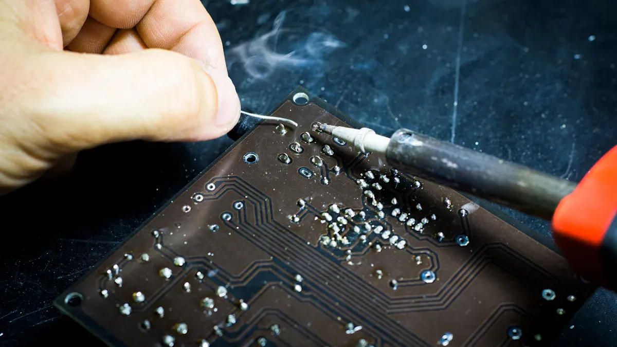
Stencil Process
You start the solder paste application by using a stencil. This stencil acts like a mask for your printed circuit board. It has small openings that match the pads on your board. You place the stencil over the board and spread solder paste across it. The paste only goes through the openings and lands on the right spots. This step is a key part of the process because it sets up the rest of your assembly work.
The stencil process helps you control where the solder goes. You avoid putting paste in the wrong places. You also make sure each pad gets the right amount. If you skip this step or do it wrong, you can cause problems later in the process. For example, you might see bridges between pads or missing connections.
Tip: Always check your stencil for damage or leftover paste before you start. A clean stencil gives you better results.
Accuracy and Quality
You need to focus on accuracy during this process. The right amount of solder paste on each pad helps you make strong and reliable joints. Too much paste can cause shorts. Too little paste can lead to weak connections. You should use machines that control the pressure and speed of the paste application. These machines help you repeat the process with the same results every time.
Quality checks matter at this stage. You can use inspection tools to look at the paste deposits. If you find mistakes, you can fix them before moving to the next process. This step saves you time and money. Good accuracy and quality in solder paste application lead to fewer problems in later steps. You get a better final product and a smoother assembly process.
Note: Careful attention to this process improves your board’s performance and reliability.
Automated PCB Assembly: Component Placement
Pick-and-Place Machines
Pick-and-place machines do the most important job in automated pcb assembly. These machines put parts on your pcb fast and with great accuracy. Using machines instead of people makes the work much quicker. Robots on the assembly line do not get tired. They move fast and do the same thing over and over without mistakes. This helps you finish more pcbs in less time.
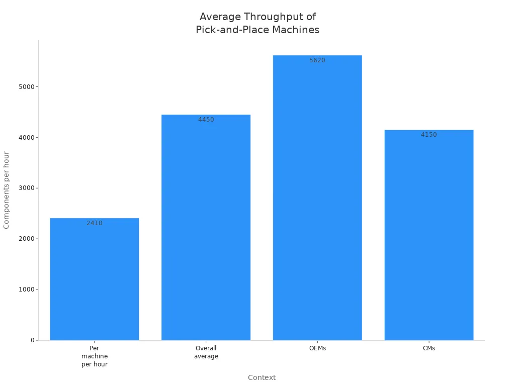
Pick-and-place robots can put up to 200,000 parts every hour. Most top machines place between 25,000 and 136,000 parts each hour. The number depends on the machine and how it is set up. Here is a table that shows how many parts different machines can place:
|
Machine Type / Context |
Throughput (components per hour) |
Notes |
|---|---|---|
|
Historical high-speed chip shooters |
Up to 53,000 |
Under best conditions |
|
Modern multi-headed, multi-gantry |
Up to 136,000 |
This is the fastest possible speed |
|
Fastest high-end machines |
Up to 200,000 |
This is the highest speed possible |
Automated pcb assembly lets your team do harder jobs. The machines take care of most of the parts. This makes your work faster and helps you finish on time.
Tip: Automated pcb assembly lines use special cameras to check each part before and after it is placed. This helps stop mistakes and makes your boards better.
Placement Precision
You need to put each part in the right spot for your pcb to work. Automated pcb assembly uses cameras and software to place parts very accurately. These machines can put parts within 0.03 mm of where they should go. People cannot be this exact by hand.
Using automated pcb assembly helps you avoid many mistakes. Problems like parts in the wrong place or facing the wrong way happen less often. The machines measure and turn parts as they work. This means less waste and more working pcbs.
Some things that cause placement mistakes are:
-
People making mistakes when placing parts by hand
-
Pick-and-place machines that are not set up right
-
Parts facing the wrong way in the tape or reel
-
Old or wrong part lists in the computer
You can stop these mistakes by doing these things:
-
Check and set up your machines often
-
Use cameras to check the parts automatically
-
Teach your workers how to use the machines well
-
Follow DFM rules when you design your board
Automated pcb assembly helps you know your parts will be placed right every time. This gives you better boards, fewer problems, and higher quality. When you use pick-and-place assembly with smt assembly, you get the best results for making lots of boards quickly.
Reflow Soldering in PCB Assembly
Heating Process
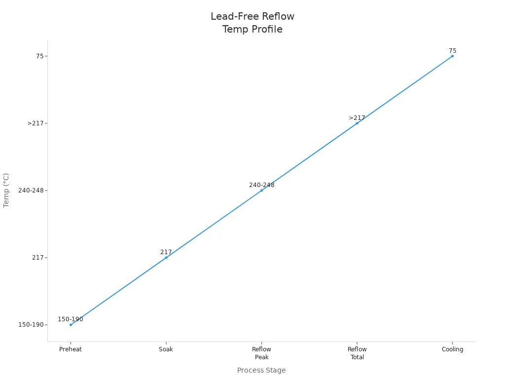
Reflow soldering is a key step in making sure your pcb works well. You use a special oven to heat the board and melt the solder paste. This process has four main stages. Each stage helps you avoid damage and get strong solder joints.
-
Preheat Zone: You slowly raise the temperature of your pcb to about 150-180°C. This takes 60-90 seconds. The slow ramp-up helps activate the flux and keeps your components safe from thermal shock.
-
Soak Zone: You keep the temperature steady between 180°C and 220°C for 60-120 seconds. This step lets the flux work fully and makes sure the whole pcb heats evenly.
-
Reflow Zone: The temperature peaks between 240°C and 260°C. The solder melts and flows, making the connections. You keep the pcb above 217°C for 30-60 seconds to get good wetting.
-
Cooling Zone: You cool the pcb down from the peak to below 50°C at a rate of 2-4°C per second. This step hardens the solder joints and stops thermal stress.
Here is a table that shows the typical temperature profile for lead-free reflow soldering:
|
Stage |
Temperature Range (°C) |
Ramp Rate (°C/s) |
Duration (s) |
Notes |
|---|---|---|---|---|
|
Preheat |
150 to 190 |
0.75 to 2 |
60 to 120 |
Gradual heating to activate flux and avoid thermal shock |
|
Soak |
~217 |
0.5 to 1 |
60 to 120 |
Flux activation, moisture removal, oxide reduction |
|
Reflow Peak |
240 to 248 |
N/A |
Peak time: 10 to 30 |
Melting solder paste, ensuring even temperature to prevent defects |
|
Reflow Total |
>217 |
N/A |
40 to 70 |
Total time in reflow zone |
|
Cooling |
From peak to 75 |
1.5 to 4 |
N/A |
Controlled cooling to solidify solder and avoid PCB warping or solder joint defects |
You can see how the temperature changes during each stage in the chart below:
Tip: Always match your reflow profile to your pcb materials and components. This helps you avoid damage and get the best results.
Solder Joint Formation
The way you control the heating process affects how well your solder joints form. If you use the right temperature profile, you get strong and reliable connections on your pcb. If you do not, you risk many problems.
-
Weak or incomplete solder joints can happen if the temperature is too low.
-
Too much heat can deform solder joints or damage the pcb insulation.
-
Uneven heating causes defects like tombstoning, where one end of a part lifts off the pad.
-
Voids may form in the solder if gases get trapped, making the joint weak.
-
Head-in-pillow defects can occur when the solder does not fully wet the pad.
You need to keep the temperature even across the pcb. Try to keep differences below 2-3°C. This helps every joint form the same way. If you control the reflow process well, you avoid warping, cracks, and other issues that lower the quality of your pcb.
Note: Good reflow soldering gives you strong, shiny solder joints and a reliable pcb that works as designed.
Quality Inspection in PCB Assembly Process
AOI and X-ray
You need special inspection tools to check your PCB assembly. AOI systems scan each board fast and look for visible problems. AOI can find up to 95% of visible issues, so it is very useful. It helps you see missing parts, wrong placements, or solder bridges. AOI works faster than people and is good for big production runs. But AOI cannot see under large parts. That is when you use X-ray inspection. X-ray looks inside the board and finds hidden solder problems. You use X-ray to check for things like voids or cold joints under chips. When you use both AOI and X-ray, you get better quality checks. These tools help you find problems early and improve your quality control.
Tip: Use AOI and X-ray together to find all types of defects and make your PCB assembly better.
Detecting Defects
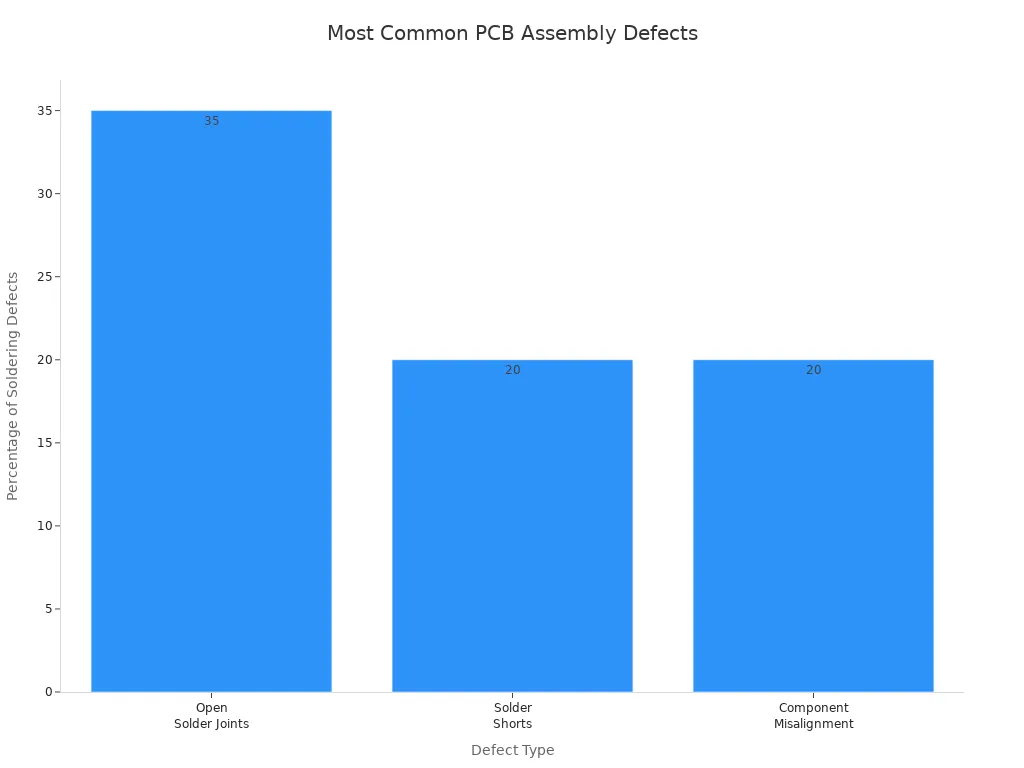
You need to know what defects to look for during inspection. Most problems happen during solder paste printing and when placing parts. Open solder joints, solder shorts, and misaligned parts are 75% of soldering problems. AOI and X-ray help you catch these before they reach customers.
Here is a table that shows the most common defects found during inspection:
|
Defect Type |
Description |
Impact/Significance |
|---|---|---|
|
Open Solder Joints |
Solder joints that fail to connect properly, causing open circuits. |
Accounts for 35% of soldering defects; leads to electrical failures. |
|
Solder Shorts |
Unintended solder connections between adjacent pads or leads. |
Represents 20% of soldering defects; causes short circuits. |
|
Component Misalignment |
Components not properly aligned with PCB pads. |
Makes up 20% of soldering defects; affects solder reliability and electrical connectivity. |
|
Cold Solder Joints |
Solder that hasn’t properly bonded, appearing dull or grainy. |
Causes poor electrical contact and reliability issues. |
|
Solder Bridges |
Excess solder creating unintended connections between pins or pads. |
Can cause short circuits and functional failures. |
|
Excess Solder |
Too much solder causing staining or bridging. |
Affects appearance and may cause shorts or assembly issues. |
|
Solder Balls |
Small solder spheres left on PCB surface. |
Potential short circuit risk and appearance defects. |
|
Missing Components |
Components absent where they should be mounted. |
Leads to open circuits and functional failures. |
|
Extra Parts |
Components placed where they should not be. |
Affects appearance and electrical performance. |
|
Reversed Polarity |
Components with polarity installed in the wrong direction. |
Severely impacts circuit functionality. |
|
Floating Components |
Components not properly seated on PCB during soldering. |
Causes mechanical and electrical reliability issues. |
|
Cracked or Broken PCB |
Physical damage causing breaks in copper traces or connections. |
Leads to malfunction and open circuits. |
|
Corrosion and Contamination |
Chemical or environmental damage affecting conductivity. |
Reduces solder reliability and causes shorts or open circuits. |
|
Solder Resist Defects |
Improper solder mask application exposing copper or causing shorts. |
Affects appearance and electrical insulation. |
|
Oxidation |
Corrosion or discoloration of solder joints or pads. |
Reduces solder joint reliability and connectivity. |
|
Warpage |
PCB bending or deformation during manufacturing. |
Affects assembly and solder joint reliability. |
|
Circuit Defects |
Damage or disconnection in PCB traces or circuits. |
Causes functional failures and reliability issues. |
You can use AOI, X-ray, and other checks to find these problems. Automated inspection works faster and better than checking by hand. These systems help you get more good boards, fix fewer mistakes, and give your customers better products.
PCB Testing and Functional Verification
In-Circuit Testing
You must check every part of your PCB before shipping. In-circuit testing, or ict test, helps with this job. Special machines test each part and connection on the board. These machines touch test points and measure if parts work right.
-
How well it works depends on your PCB design. If you add more test points and use design for testability, you get better results.
-
Boards with tiny or crowded layouts may have less coverage because there is not much space for test points.
-
ict test works best when you use it with AOI, X-ray, or flying probe testing.
Tip: Add test points early in your design. This makes in-circuit testing quicker and more correct.
Functional Testing
After ict test, you must see if your PCB works in real life. Functional testing checks if your board does its job. You run the board through real tasks and stress tests. This helps you find open circuits, short circuits, or cold solder joints before customers get your product.
|
Test Aspect |
Fault Detected |
Impact on Product |
Outcome of Function Test |
|---|---|---|---|
|
Open circuit in trace |
Device fails to power on |
Fault found early, repair before shipment |
|
|
Solder Joint Check |
Cold solder joint |
Poor connection, intermittent failures |
Issue fixed, prevents malfunction in the field |
|
Component Placement Check |
Misplaced component |
Wrong device function |
Corrected, ensures proper operation |
|
Short Circuit Test |
Short between components |
Device may fail during use |
Fault detected, avoids field failure |
Functional testing helps lower the number of failures in the field. Studies show this step can catch up to 70% of problems. You can see 30% fewer failures after using function test. Solder joint checks can cut failures by 40%. If you add compliance testing, you lower failures even more. Your products become safer and more reliable for customers.
Note: Good testing and function test help your products last longer and stop costly returns.
Selective Soldering for Through-Hole Components
Manual vs. Automated
You have two ways to do selective soldering. One way is manual soldering. Skilled workers use soldering irons to connect through-hole components. The other way is automated selective soldering. Machines do the work and control each step very carefully. Automation gives you much better results. Automated selective soldering keeps defects very low, under 10 DPMO. Manual soldering often has more than 500 DPMO. This big gap happens because machines are more steady and careful. Machines watch every step, so you get fewer problems like bad hole fill or solder bridges. Manual soldering can have more mistakes because people get tired or miss small things. If you want your assembly to be high quality with fewer errors, automated selective soldering is the best choice.
Tip: Using automated selective soldering makes your boards better and saves money on fixing mistakes.
Application Scenarios
Selective soldering is best for some special jobs. You should use it when other ways do not work well. Here are some times to use selective soldering:
-
Tall parts block heat in wave soldering.
-
Thick boards or heavy copper make hand soldering tough.
-
Parts are close together, so wave soldering tools do not fit.
-
Big connectors with lots of pins are hard to solder by hand.
-
You need to set up machines for tricky pin layouts.
-
You want every solder joint to look the same every time.
Selective soldering is good when you need careful control. You can program the machine for boards with many different parts. It helps when you have both surface mount and through-hole parts close together. You do not overheat sensitive parts. You get strong and reliable joints. Selective soldering makes your work faster and your boards better.
Note: Pick selective soldering if your board needs special care that wave or hand soldering cannot give.
Final Assembly and Inspection
Mechanical Assembly
This is the last step in putting your board together. You add things like connectors, shields, heat sinks, and mounting hardware. These parts help your PCB fit inside its case. You need to be gentle with each board. Static electricity or rough handling can hurt it. Always use the right tools and follow the steps in the instructions. If you skip a step or hurry, you might break small parts or put things in the wrong place.
Check that screws, clips, and fasteners are tight but not too tight. Loose parts can shake or cause electrical trouble. If you use too much force, you can crack the board or break solder joints. Good assembly helps your product last longer and work better.
Tip: Wear special wrist straps and use grounded tables. This keeps your boards safe from static electricity.
Final Quality Checks
You need to test and check your board before you ship it. This step helps you find any last problems. It also makes sure your board meets all the rules. Use your eyes and machines to look for these issues:
-
Parts that are not straight or are broken
-
Tombstoning, when parts stand up on one end
-
Cracked parts from too much heat
-
Weak solder or too much paste
-
Pads that lift up or do not get enough solder
-
Damage from static electricity
-
Dirty boards with leftover paste or dirt
You might use x-ray tools to find hidden problems like head-in-pillow or QFN voids. If you find a problem, you may need to fix the board. Fixing takes more work, parts, and time. This can slow down your work and cost more money. Sometimes, fixing a board can cause new problems or make you late.
|
Cost Factor |
Description |
Impact on Costs and Operations |
|---|---|---|
|
Labor, Equipment, Parts |
More work and parts needed to fix boards |
|
|
Time-Consuming Process |
Fixing can take a long time |
Slower work, missed deadlines |
|
Skill and Expertise Gaps |
Needs trained workers and special tools |
More mistakes, expensive repairs |
|
Quality Assurance Risks |
Bad fixes may miss problems |
Broken products, unhappy customers |
You can stop most problems by checking and testing carefully at the end. Good checks help you send out strong products and keep your customers happy.
Note: Careful final testing and checks help your work go faster and keep your customers smiling. 🛡️
You get strong PCBs when you follow every step carefully. Good teamwork at the start and careful soldering help stop mistakes. This also makes your boards last longer. Experts use special inspection tools and trained workers. This means fewer problems and better boards.
-
Rules like IPC-A-610 and ISO 9001 tell you how to make good boards.
-
Machines and regular tests help find problems early.
-
Working with certified companies gives you better tools and skilled people.
Pick good methods and trusted helpers to make your projects better and more reliable. 🛠️
FAQ
What is the most important step in PCB assembly?
You need to focus on every step, but careful design and planning help you avoid most problems. Good preparation makes the rest of the process smoother and improves your final product.
How does automated pcb assembly improve quality?
Automated pcb assembly uses machines to place parts with high accuracy. You get fewer mistakes and faster production. This method helps you make more reliable boards.
Why do you need testing after assembly?
Testing helps you find problems before you ship your product. You can check if every part works and if the board meets your requirements. This step protects your reputation and saves money.
Can you fix mistakes after assembly?
You can repair some mistakes, like bad solder joints or missing parts. Fixing takes extra time and skill. Careful checks during each step help you avoid most errors.
How do you choose the right PCB design?
You should match your design to your product’s needs. Think about size, shape, and how many parts you need. Good design makes assembly easier and improves reliability.